SBAS444D May   2009  – January 2018 ADS1113 , ADS1114 , ADS1115

PRODUCTION DATA.  

  1. Features
  2. Applications
  3. Description
    1.     Device Images
      1.      Simplified Block Diagrams
  4. Revision History
  5. Device Comparison Table
  6. Pin Configuration and Functions
    1.     Pin Functions
  7. Specifications
    1. 7.1 Absolute Maximum Ratings
    2. 7.2 ESD Ratings
    3. 7.3 Recommended Operating Conditions
    4. 7.4 Thermal Information
    5. 7.5 Electrical Characteristics
    6. 7.6 Timing Requirements: I2C
    7. 7.7 Typical Characteristics
  8. Parameter Measurement Information
    1. 8.1 Noise Performance
  9. Detailed Description
    1. 9.1 Overview
    2. 9.2 Functional Block Diagrams
    3. 9.3 Feature Description
      1. 9.3.1 Multiplexer
      2. 9.3.2 Analog Inputs
      3. 9.3.3 Full-Scale Range (FSR) and LSB Size
      4. 9.3.4 Voltage Reference
      5. 9.3.5 Oscillator
      6. 9.3.6 Output Data Rate and Conversion Time
      7. 9.3.7 Digital Comparator (ADS1114 and ADS1115 Only)
      8. 9.3.8 Conversion Ready Pin (ADS1114 and ADS1115 Only)
      9. 9.3.9 SMbus Alert Response
    4. 9.4 Device Functional Modes
      1. 9.4.1 Reset and Power-Up
      2. 9.4.2 Operating Modes
        1. 9.4.2.1 Single-Shot Mode
        2. 9.4.2.2 Continuous-Conversion Mode
      3. 9.4.3 Duty Cycling For Low Power
    5. 9.5 Programming
      1. 9.5.1 I2C Interface
        1. 9.5.1.1 I2C Address Selection
        2. 9.5.1.2 I2C General Call
        3. 9.5.1.3 I2C Speed Modes
      2. 9.5.2 Slave Mode Operations
        1. 9.5.2.1 Receive Mode
        2. 9.5.2.2 Transmit Mode
      3. 9.5.3 Writing To and Reading From the Registers
      4. 9.5.4 Data Format
    6. 9.6 Register Map
      1. 9.6.1 Address Pointer Register (address = N/A) [reset = N/A]
        1. Table 6. Address Pointer Register Field Descriptions
      2. 9.6.2 Conversion Register (P[1:0] = 0h) [reset = 0000h]
        1. Table 7. Conversion Register Field Descriptions
      3. 9.6.3 Config Register (P[1:0] = 1h) [reset = 8583h]
        1. Table 8. Config Register Field Descriptions
      4. 9.6.4 Lo_thresh (P[1:0] = 2h) [reset = 8000h] and Hi_thresh (P[1:0] = 3h) [reset = 7FFFh] Registers
        1. Table 9. Lo_thresh and Hi_thresh Register Field Descriptions
  10. 10Application and Implementation
    1. 10.1 Application Information
      1. 10.1.1 Basic Connections
      2. 10.1.2 Single-Ended Inputs
      3. 10.1.3 Input Protection
      4. 10.1.4 Unused Inputs and Outputs
      5. 10.1.5 Analog Input Filtering
      6. 10.1.6 Connecting Multiple Devices
      7. 10.1.7 Quickstart Guide
    2. 10.2 Typical Application
      1. 10.2.1 Design Requirements
      2. 10.2.2 Detailed Design Procedure
        1. 10.2.2.1 Shunt Resistor Considerations
        2. 10.2.2.2 Operational Amplifier Considerations
        3. 10.2.2.3 ADC Input Common-Mode Considerations
        4. 10.2.2.4 Resistor (R1, R2, R3, R4) Considerations
        5. 10.2.2.5 Noise and Input Impedance Considerations
        6. 10.2.2.6 First-order RC Filter Considerations
        7. 10.2.2.7 Circuit Implementation
        8. 10.2.2.8 Results Summary
      3. 10.2.3 Application Curves
  11. 11Power Supply Recommendations
    1. 11.1 Power-Supply Sequencing
    2. 11.2 Power-Supply Decoupling
  12. 12Layout
    1. 12.1 Layout Guidelines
    2. 12.2 Layout Example
  13. 13Device and Documentation Support
    1. 13.1 Documentation Support
      1. 13.1.1 Related Documentation
    2. 13.2 Related Links
    3. 13.3 Receiving Notification of Documentation Updates
    4. 13.4 Community Resources
    5. 13.5 Trademarks
    6. 13.6 Electrostatic Discharge Caution
    7. 13.7 Glossary
  14. 14Mechanical, Packaging, and Orderable Information

Package Options

Mechanical Data (Package|Pins)
Thermal pad, mechanical data (Package|Pins)
Orderable Information

Connecting Multiple Devices

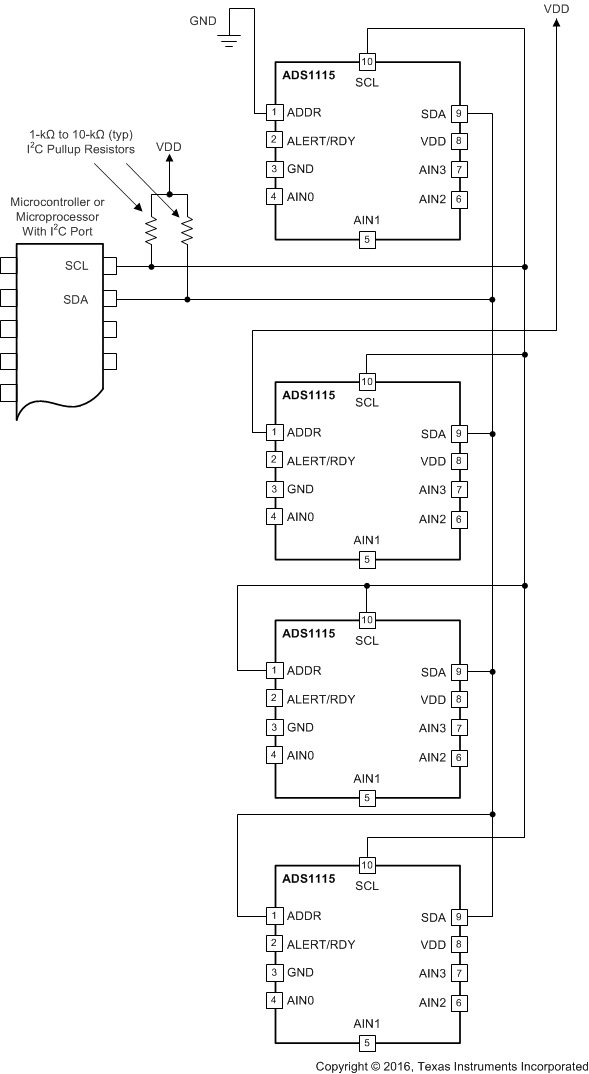
It is possible to connect up to four ADS111x devices to a single I2C bus using different address pin configurations for each device. Use the address pin to set the ADS111x to one of four different I2C addresses. Use the GND, VDD and SCL addresses first. If SDA is used as the device address, hold the SDA line low for at least 100 ns after the SCL line goes low to make sure the device decodes the address correctly during I2C communication. An example showing four ADS111x devices on the same I2C bus is shown in Figure 42. One set of pullup resistors is required per bus. The pullup resistor values may need to be lowered to compensate for the additional bus capacitance presented by multiple devices and increased line length.
ADS1113 ADS1114 ADS1115 ai_multi_ads_connex_bas444.gif

NOINDENT:

NOTE: ADS111x power and input connections omitted for clarity. The ADDR pin selects the I2C address.
Figure 42. Connecting Multiple ADS111x Devices