SBAS790C October   2018  – June 2019 ADS125H02

PRODUCTION DATA.  

  1. Features
  2. Applications
  3. Description
    1.     Functional Block Diagram
  4. Revision History
  5. Device Comparison Table
  6. Pin Configuration and Functions
    1.     Pin Functions
  7. Specifications
    1. 7.1 Absolute Maximum Ratings
    2. 7.2 ESD Ratings
    3. 7.3 Recommended Operating Conditions
    4. 7.4 Thermal Information
    5. 7.5 Electrical Characteristics
    6. 7.6 Timing Requirements
    7. 7.7 Switching Characteristics
    8. 7.8 Typical Characteristics
  8. Parameter Measurement Information
    1. 8.1 Noise Performance
  9. Detailed Description
    1. 9.1 Overview
    2. 9.2 Functional Block Diagram
    3. 9.3 Feature Description
      1. 9.3.1 Input Range
      2. 9.3.2 Analog Inputs
        1. 9.3.2.1 ESD Diodes
        2. 9.3.2.2 Input Multiplexer
          1. 9.3.2.2.1 Analog Inputs (AIN0, AIN1, AINCOM)
          2. 9.3.2.2.2 High-Voltage Power Supply Readback
          3. 9.3.2.2.3 Internal VCOM Connection (Default)
          4. 9.3.2.2.4 Temperature Sensor
      3. 9.3.3 Programmable Gain Amplifier (PGA)
        1. 9.3.3.1 PGA Operating Range
        2. 9.3.3.2 PGA Monitor
      4. 9.3.4 Reference Voltage
        1. 9.3.4.1 Internal Reference
        2. 9.3.4.2 External Reference
        3. 9.3.4.3 AVDD Power-Supply Reference
        4. 9.3.4.4 Reference Monitor
      5. 9.3.5 Current Sources (IDAC1 and IDAC2)
      6. 9.3.6 General-Purpose Inputs and Outputs (GPIOs)
      7. 9.3.7 ADC Modulator
      8. 9.3.8 Digital Filter
        1. 9.3.8.1 Sinc Filter Mode
          1. 9.3.8.1.1 Sinc Filter Frequency Response
        2. 9.3.8.2 FIR Filter
        3. 9.3.8.3 50-Hz and 60-Hz Normal Mode Rejection
    4. 9.4 Device Functional Modes
      1. 9.4.1 Conversion Control
        1. 9.4.1.1 Continuous-Conversion Mode
        2. 9.4.1.2 Pulse-Conversion Mode
        3. 9.4.1.3 Conversion Latency
        4. 9.4.1.4 Start-Conversion Delay
      2. 9.4.2 Auto-Zero Mode
      3. 9.4.3 Clock Mode
      4. 9.4.4 Reset
        1. 9.4.4.1 Power-On Reset
        2. 9.4.4.2 Reset by Pin
        3. 9.4.4.3 Reset by Command
      5. 9.4.5 Calibration
        1. 9.4.5.1 Offset and Full-Scale Calibration
          1. 9.4.5.1.1 Offset Calibration Registers
          2. 9.4.5.1.2 Full-Scale Calibration Registers
        2. 9.4.5.2 Offset Calibration (OFSCAL)
        3. 9.4.5.3 Full-Scale Calibration (GANCAL)
        4. 9.4.5.4 Calibration Command Procedure
        5. 9.4.5.5 User Calibration Procedure
    5. 9.5 Programming
      1. 9.5.1 Serial Interface
        1. 9.5.1.1 Chip-Select Pins (CS1 and CS2)
        2. 9.5.1.2 Serial Clock (SCLK)
        3. 9.5.1.3 Data Input (DIN)
        4. 9.5.1.4 Data Output/Data Ready (DOUT/DRDY)
      2. 9.5.2 Data Ready (DRDY)
        1. 9.5.2.1 DRDY in Continuous-Conversion Mode
        2. 9.5.2.2 DRDY in Pulse-Conversion Mode
        3. 9.5.2.3 Data Ready by Software Polling
      3. 9.5.3 Conversion Data
        1. 9.5.3.1 Status Byte (STATUS0)
        2. 9.5.3.2 Conversion Data Format
      4. 9.5.4 Cyclic Redundancy Check (CRC)
      5. 9.5.5 Commands
        1. 9.5.5.1  General Command Format
        2. 9.5.5.2  NOP Command
        3. 9.5.5.3  RESET Command
        4. 9.5.5.4  START Command
        5. 9.5.5.5  STOP Command
        6. 9.5.5.6  RDATA Command
        7. 9.5.5.7  OFSCAL Command
        8. 9.5.5.8  GANCAL Command
        9. 9.5.5.9  RREG Command
        10. 9.5.5.10 WREG Command
        11. 9.5.5.11 LOCK Command
        12. 9.5.5.12 UNLOCK Command
    6. 9.6 Register Map
      1. 9.6.1  Device Identification (ID) Register (address = 00h) [reset = 6xh]
        1. Table 30. ID Register Field Descriptions
      2. 9.6.2  Main Status (STATUS0) Register (address = 01h) [reset = 01h]
        1. Table 31. STATUS0 Register Field Descriptions
      3. 9.6.3  Mode 0 (MODE0) Register (address = 02h) [reset = 24h]
        1. Table 32. MODE0 Register Field Descriptions
      4. 9.6.4  Mode 1 (MODE1) Register (address = 03h) [reset = 01h]
        1. Table 33. MODE1 Register Field Descriptions
      5. 9.6.5  Mode 2 (MODE2) Register (address = 04h) [reset = 00h]
        1. Table 34. MODE2 Register Field Descriptions
      6. 9.6.6  Mode 3 (MODE3) Register (address = 05h) [reset = 00h]
        1. Table 35. MODE3 Register Field Descriptions
      7. 9.6.7  Reference Configuration (REF) Register (address = 06h) [reset = 05h]
        1. Table 36. REF Register Field Descriptions
      8. 9.6.8  Offset Calibration (OFCALx) Registers (address = 07h, 08h, 09h) [reset = 00h, 00h, 00h]
        1. Table 37. OFCAL0, OFCAL1, OFCAL2 Registers Field Description
      9. 9.6.9  Full-Scale Calibration (FSCALx) Registers (address = 0Ah, 0Bh, 0Ch) [reset = 00h, 00h, 40h]
        1. Table 38. FSCAL0, FSCAL1, FSCAL2 Registers Field Description
      10. 9.6.10 Current Source Multiplexer (I_MUX) Register (address = 0Dh) [reset = FFh]
        1. Table 39. I_MUX Register Field Descriptions
      11. 9.6.11 Current Source Magnitude (I_MAG) Register (address = 0Eh) [reset = 00h]
        1. Table 40. I_MAG Register Field Descriptions
      12. 9.6.12 Reserved (RESERVED) Register (address = 0Fh) [reset = 00h]
        1. Table 41. RESERVED Register Field Descriptions
      13. 9.6.13 MODE4 (MODE4) Register (address = 10h) [reset = 50h]
        1. Table 42. MODE4 Register Field Descriptions
      14. 9.6.14 PGA Alarm (STATUS1) Register (address = 11h) [reset = xxh]
        1. Table 43. STATUS1 Register Field Descriptions
      15. 9.6.15 Status 2 (STATUS2) Register (address = 12h) [reset = 0xh]
        1. Table 44. STATUS2 Register Field Descriptions
  10. 10Application and Implementation
    1. 10.1 Application Information
      1. 10.1.1 Input Range
      2. 10.1.2 Input Overload
        1. 10.1.2.1 Input Signal Rate of Change (dV/dt)
      3. 10.1.3 Unused Inputs and Outputs
    2. 10.2 Typical Applications
      1. 10.2.1 ±10-V Analog Input Module
        1. 10.2.1.1 Design Requirements
        2. 10.2.1.2 Detailed Design Procedure
        3. 10.2.1.3 Application Curves
      2. 10.2.2 Thermocouple Input With High Common-Mode Voltage
    3. 10.3 Initialization Setup
  11. 11Power Supply Recommendations
    1. 11.1 Power-Supply Decoupling
    2. 11.2 Analog Power-Supply Clamp
    3. 11.3 Power-Supply Sequencing
    4. 11.4 5-V to ±15-V DC-DC Converter
  12. 12Layout
    1. 12.1 Layout Guidelines
    2. 12.2 Layout Example
  13. 13Device and Documentation Support
    1. 13.1 Documentation Support
      1. 13.1.1 Related Documentation
    2. 13.2 Receiving Notification of Documentation Updates
    3. 13.3 Community Resources
    4. 13.4 Trademarks
    5. 13.5 Electrostatic Discharge Caution
    6. 13.6 Glossary
  14. 14Mechanical, Packaging, and Orderable Information

Package Options

Mechanical Data (Package|Pins)
Thermal pad, mechanical data (Package|Pins)
Orderable Information

±10-V Analog Input Module

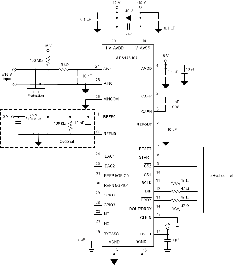
Figure 98 illustrates an example of the ADS125H02 used in a ±10-V analog input programmable logic controller (PLC) module. The inputs of the ADC are protected by external ESD diodes to provide system-level protection. A 100-MΩ resistor is used to pull the positive analog input to 15 V if the field-wiring connection is open or the transmitter has failed in open-circuit mode.

The signal from the transmitter is filtered to remove EMI and RFI interference when operated in noisy environments. The resistor also acts to limit the input current in the event of an input overvoltage, including if the module loses power with the signal present. The negative input signal is connected to AIN0, which is also connected to AGND. Connection to AGND is necessary if the sensor power supply is not referenced to the ADC ground.

The ADC measures the differential voltage between inputs AIN1 and AIN0. The input configuration is single-ended with the input voltage driven ±10 V relative to AIN0 (AGND).

Operation by internal reference requires a 10-µF capacitor connected to the REFOUT pin. Otherwise, apply the external reference voltage to REFP0 and REFN0. A 100-kΩ resistor biases the differential reference voltage to 0 V. The resistor provides the bias to allow the reference monitor to detect a failed or missing reference voltage that otherwise may be unnoticed.

Because the excitation current sources and GPIOs are not used they are left unconnected.

The internal oscillator is selected by connecting the CLKIN input pin to ground. The serial interface and digital control lines of the ADC are connected to the host.

The zener diode clamps the high-voltage supply (HV_AVDD – HV_AVSS) to 40 V to provide overvoltage protection if an input signal is present with module power off.
ADS125H02 ads125h02-typical-application.gifFigure 98. ±10-V Analog Input PLC Module