SNAS602C FEBRUARY 2013 – December 2014 ADS1293
PRODUCTION DATA.
- 1 Features
- 2 Applications
- 3 Description
- 4 Application Diagram
- 5 Revision History
- 6 Pin Configuration and Functions
- 7 Specifications
-
8 Detailed Description
- 8.1 Overview
- 8.2 Functional Block Diagram
- 8.3
Feature Description
- 8.3.1 Flexible Routing Switch
- 8.3.2 Battery Monitoring
- 8.3.3 Test Mode
- 8.3.4 Analog Front-End
- 8.3.5 Instrumentation Amplifier (INA)
- 8.3.6 Sigma-Delta Modulator (SDM)
- 8.3.7 Programmable Digital Filters
- 8.3.8 Filter Settling Time
- 8.3.9 Analog Pace Channel
- 8.3.10 Wilson Reference
- 8.3.11 Common-Mode (CM) Detector
- 8.3.12 Right-Leg Drive (RLD)
- 8.3.13 Capacitive Load Driving
- 8.3.14 Error Status: RLD Rail
- 8.3.15 Lead-Off Detection (LOD)
- 8.3.16 DC Lead-Off Detect
- 8.3.17 Analog AC Lead-Off Detect
- 8.3.18 Digital AC Lead-Off Detect
- 8.3.19 Clock Oscillator
- 8.3.20 Synchronization
- 8.3.21 Single-Chip Multi-Channel Synchronization
- 8.3.22 Multichip Synchronization
- 8.3.23 Synchronization Errors
- 8.3.24 Alarm Functions
- 8.3.25 Error Filtering
- 8.3.26 ALARMB Pin and Error Masking
- 8.3.27 Error Register Automatic Clearing Description
- 8.3.28 Alarm Propagation
- 8.3.29 Reference Voltage Generators
- 8.3.30 Power Management
- 8.4 Device Functional Modes
- 8.5 Programming
- 8.6
Register Maps
- 8.6.1 Operation Mode Registers
- 8.6.2 Input Channel Selection Registers
- 8.6.3 Lead-Off Detect Control Registers
- 8.6.4 Common-Mode Detection and Right-Leg Drive Common-Mode Feedback Control Registers
- 8.6.5 Wilson Control Registers
- 8.6.6 Reference Registers
- 8.6.7 OSC Control Registers
- 8.6.8 AFE Control Registers
- 8.6.9 Error Status Registers
- 8.6.10 Digital Registers
- 8.6.11 Pace and ECG Data Read Back Registers
- 9 Application and Implementation
- 10Power Supply Recommendations
- 11Layout
- 12Device and Documentation Support
- 13Mechanical, Packaging, and Orderable Information
Package Options
Mechanical Data (Package|Pins)
- RSG|28
Thermal pad, mechanical data (Package|Pins)
Orderable Information
9 Application and Implementation
NOTE
Information in the following applications sections is not part of the TI component specification, and TI does not warrant its accuracy or completeness. TI’s customers are responsible for determining suitability of components for their purposes. Customers should validate and test their design implementation to confirm system functionality.
9.1 Application Information
The ADS1293 is an AFE for biopotential measurements. The device is typically used in portable, low-power medical, sports, and fitness ECG applications. The device's flexibility and synchronization features allows it to be used it in configurations that range from single-chip/single-channel applications to multi-chip/multi-channel applications. The following sections will explore the use model in some of these configurations.
9.2 Typical Applications
9.2.1 3-Lead ECG Application
In the 3-Lead ECG example shown in Figure 84, the right-arm (RA), left-arm (LA), left-leg (LL) and right-leg (RL) electrodes are connected to the IN1, IN2, IN3 and IN4 pins. The ADS1293 uses the Common-Mode Detector to measure the common-mode of the system by averaging the voltage of input pins IN1, IN2 and IN3, and uses this signal in the right-leg drive feedback circuit
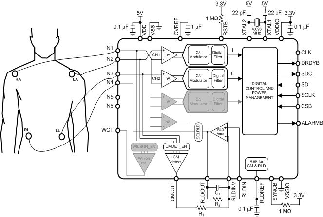 Figure 84. 3-Lead ECG Application
9.2.1.1 Design Requirements
For this design example, use the parameters listed in Table 12 as the set-up parameters.
Table 12. Design Parameters
| DESIGN PARAMETER | EXAMPLE VALUE |
|---|---|
| Number of electrodes | 4 |
| Lead I definition | LA – RA |
| Lead II definition | LL –RA |
| Bandwidth | 175 Hz |
| Output data rate | 853 sps |
| Analog supply voltage | 5.0 V |
| Digital I/O supply voltage | 3.3 V |
9.2.1.2 Detailed Design Procedure
Follow the next steps to configure the device for this example, starting from default registers values.
- Set address 0x01 = 0x11: Connect channel 1’s INP to IN2 and INN to IN1.
- Set address 0x02 = 0x19: Connect channel 2’s INP to IN3 and INN to IN1.
- Set address 0x0A = 0x07: Enable the common-mode detector on input pins IN1, IN2 and IN3.
- Set address 0x0C = 0x04: Connect the output of the RLD amplifier internally to pin IN4.
- Set address 0x12 = 0x04: Use external crystal and feed the internal oscillator's output to the digital.
- Set address 0x14 = 0x24: Shuts down unused channel 3’s signal path.
- Set address 0x21 = 0x02: Configures the R2 decimation rate as 5 for all channels.
- Set address 0x22 = 0x02: Configures the R3 decimation rate as 6 for channel 1.
- Set address 0x23 = 0x02: Configures the R3 decimation rate as 6 for channel 2.
- Set address 0x27 = 0x08: Configures the DRDYB source to channel 1 ECG (or fastest channel).
- Set address 0x2F = 0x30: Enables channel 1 ECG and channel 2 ECG for loop read-back mode.
- Set address 0x00 = 0x01: Starts data conversion.
Follow the description in the Streaming section to read the data. The ADS1293 will measure lead I and lead II. Lead III can be calculated as follows: Lead III = Lead II – Lead I
Optionally, the third channel could be used to measure Lead III.
9.2.1.3 Application Curves
Figure 85 show measurement data collected by a single ADS1293 device connected to an ECG simulator configured to produce an ECG signals at a rate of 60 per minute and with an amplitude of 2 mV. The data was collected simultaneously by channels 1 and 2 of the device during a period of 10 seconds.
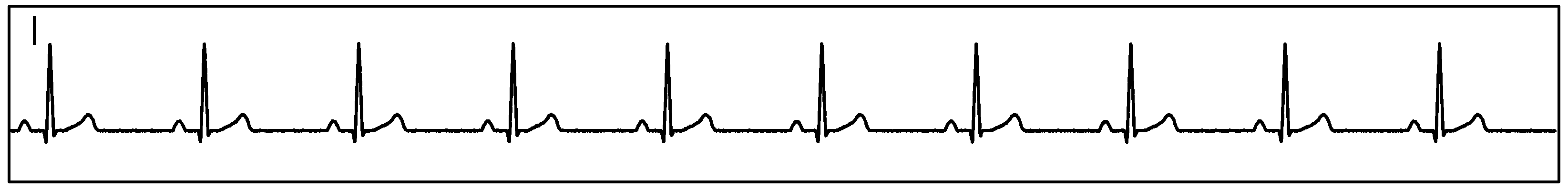
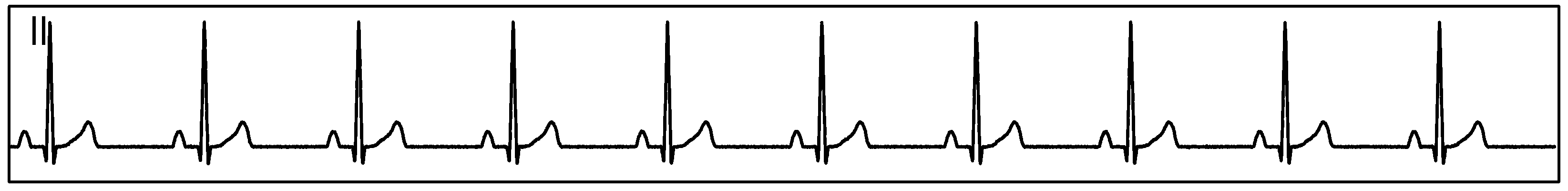 Figure 85. Single ADS1293 Device With an ECG Simulator, CH1 and CH2: ECG Signals
9.2.2 5-Lead ECG Application
In the 5-Lead ECG example shown in Figure 86, the ADS1293 uses the Common-Mode Detector to measure the common-mode of the system by averaging the voltage of input pins IN1, IN2 and IN3, and uses this signal in the right-leg drive feedback circuit
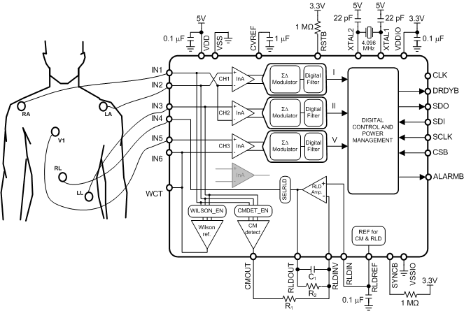 Figure 86. 5-Lead ECG Application
9.2.2.1 Design Requirements
For this design example, use the parameters listed in Table 13 as the setup parameters.
Table 13. Design Parameters
| DESIGN PARAMETER | EXAMPLE VALUE |
|---|---|
| Number of electrodes | 5 |
| Lead I definition | LA – RA |
| Lead II definition | LL –RA |
| Lead V definition | V1 – WCT |
| Bandwidth | 175 Hz |
| Output data rate | 853 sps |
| Analog supply voltage | 5.0 V |
| Digital I/O supply voltage | 3.3 V |
9.2.2.2 Detailed Design Procedure
The following steps configure the ADS1293 for a 5-lead application with an ECG bandwidth of 175 Hz and an output data rate of 853 Hz; it is assumed that the device registers contain their default power-up values.
- Set address 0x01 = 0x11: Connects channel 1’s INP to IN2 and INN to IN1.
- Set address 0x02 = 0x19: Connect channel 2’s INP to IN3 and INN to IN1.
- Set address 0x03 = 0x2E: Connects channel 3’s INP to IN5 and INN to IN6.
- Set address 0x0A = 0x07: Enables the common-mode detector on input pins IN1, IN2 and IN3.
- Set address 0x0C = 0x04: Connects the output of the RLD amplifier internally to pin IN4.
- Set addresses 0x0D = 0x01, 0x0E = 0x02, 0x0F = 0x03: Connects the first buffer of the Wilson reference to the IN1 pin, the second buffer to the IN2 pin, and the third buffer to the IN3 pin.
- Set address 0x10 = 0x01: Connects the output of the Wilson reference internally to IN6.
- Set address 0x12 = 0x04: Uses external crystal and feeds the output of the internal oscillator module to the digital.
- Set address 0x21 = 0x02: Configures the R2 decimation rate as 5 for all channels.
- Set address 0x22 = 0x02: Configures the R3 decimation rate as 6 for channel 1.
- Set address 0x23 = 0x02: Configures the R3 decimation rate as 6 for channel 2.
- Set address 0x24 = 0x02: Configures the R3 decimation rate as 6 for channel 3.
- Set address 0x27 = 0x08: Configures the DRDYB source to ECG channel 1 (or fastest channel).
- Set address 0x2F = 0x70: Enables ECG channel 1, ECG channel 2, and ECG channel 3 for loop read-back mode.
- Set address 0x00 = 0x01: Starts data conversion.
Follow the description in the Streaming section to read the data.
9.2.2.3 Application Curves
Figure 87 show measurement data collected by a single ADS1293 device connected to an ECG simulator configured to produce an ECG signals at a rate of 60 per minute and with an amplitude of 2 mV. The data was collected simultaneously by channels 1, 2 and 3 of the device during a period of 10 seconds.
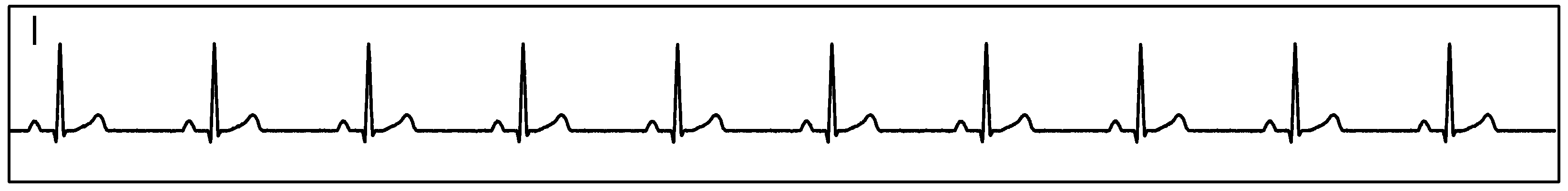
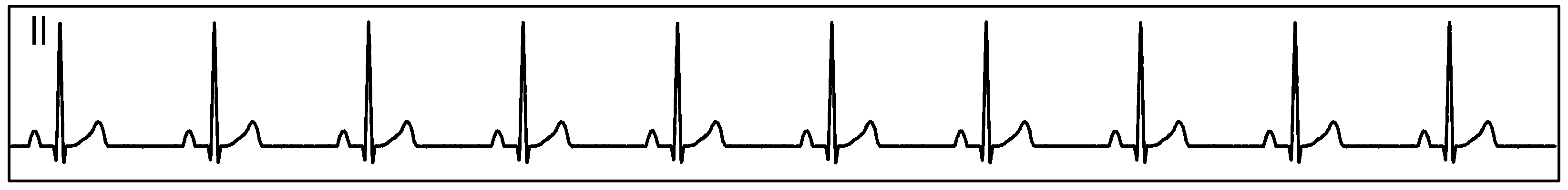
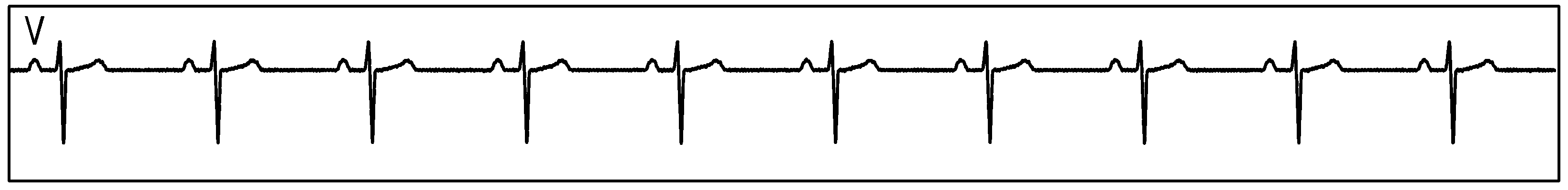 Figure 87. Single ADS1293 Device With an ECG Simulator, CH1, CH2, and CH3: ECG Signals
9.2.3 8- or 12-Lead ECG Application
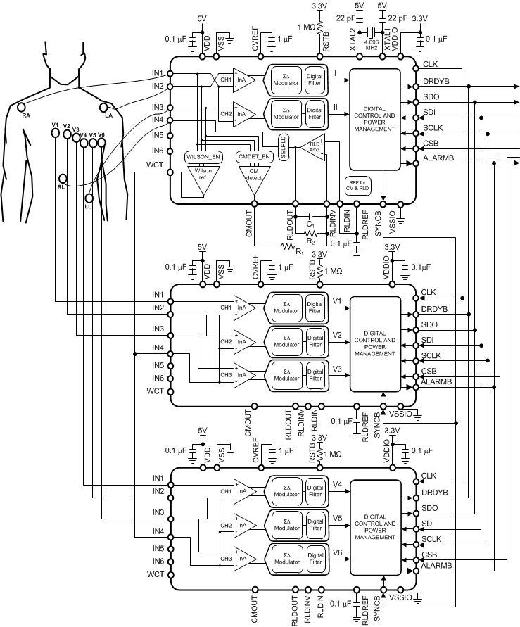 Figure 88. 8- or 12-Lead ECG Application
Figure 88 shows the ADS1293 master/slave setup for an 8-Lead to 12-Lead ECG system. The ADS1293 uses the Common-Mode Detector to measure the common-mode of the system by averaging the voltage of input pins IN1, IN2 and IN3, and uses this signal in the right-leg drive feedback circuit
9.2.3.1 Design Requirements
For this design example, use the parameters listed in Table 14 as the setup parameters.
Table 14. Design Parameters
| DESIGN PARAMETER | EXAMPLE VALUE |
|---|---|
| Number of electrodes | 10 |
| Lead I definition | LA – RA |
| Lead II definition | LL –RA |
| Lead V1 definition | V1 – WCT |
| Lead V2 definition | V2 – WCT |
| Lead V3 definition | V3 – WCT |
| Lead V4 definition | V4 – WCT |
| Lead V5 definition | V5 – WCT |
| Lead V6 definition | V6 – WCT |
| Bandwidth | 175 Hz |
| Output data rate | 853 sps |
| Analog supply voltage | 5.0 V |
| Digital I/O supply voltage | 3.3 V |
9.2.3.2 Detailed Design Procedure
The next steps will configure the master device; it is assumed that the device registers contain their default power-up values.
- Set address 0x01 = 0x11: Connects channel 1’s INP to IN2 and INN to IN1.
- Set address 0x02 = 0x19: Connect channel 2’s INP to IN3 and INN to IN1.
- Set address 0x0A = 0x07: Enables the common-mode detector on input pins IN1, IN2 and IN3.
- Set address 0x0C = 0x04: Connects the output of the RLD amplifier internally to pin IN4.
- Set addresses 0x0D = 0x01, 0x0E = 0x02, 0x0F = 0x03: Connects the first buffer of the Wilson reference to the IN1 pin, the second buffer to the IN2 pin, and the third buffer to the IN3 pin.
- Set address 0x12 = 0x05: Uses external crystal, feeds the output of the internal oscillator module to the digital, and enables the CLK pin output driver
- Set address 0x14 = 0x24: Shuts down unused channel 3’s signal path.
- Set address 0x21 = 0x02: Configures the R2 decimation rate as 5 for all channels.
- Set address 0x22 = 0x02: Configures the R3 decimation rate as 6 for channel 1.
- Set address 0x23 = 0x02: Configures the R3 decimation rate as 6 for channel 2.
- Set address 0x27 = 0x08: Configures the data-ready source to channel 1 ECG (or fastest channel).
- Set address 0x28 = 0x08: Configures the synchronization source to channel 1 ECG (or slowest channel).
- Set address 0x2F = 0x30: Enables ECG channel 1 and ECG channel 2 for loop read-back mode.
- Set address 0x01 = 0x0C: Connects channel 1’s INP to IN1 and INN to IN4.
- Set address 0x02 = 0x14: Connects channel 2’s INP to IN2 and INN to IN4.
- Set address 0x03 = 0x1C: Connects channel 3’s INP to IN3 and INN to IN4.
- Set address 0x12 = 0x06: Uses external clock signal on the CLK pin and feeds it to the digital.
- Set address 0x21 = 0x02: Configures the R2 decimation rate as 5 for all channels.
- Set address 0x22 = 0x02: Configures the R3 decimation rate as 6 for channel 1.
- Set address 0x23 = 0x02: Configures the R3 decimation rate as 6 for channel 2.
- Set address 0x24 = 0x02: Configures the R3 decimation rate as 6 for channel 3.
- Set address 0x27 = 0x00: DRDYB pin not asserted by slave devices.
- Set address 0x28 = 0x40: Disables SYNCB driver and configures pin as input.
- Set address 0x2F = 0x70: Enables ECG channel 1, ECG channel 2, and ECG channel 3 for loop read-back mode.
- Set address 0x00 = 0x01: Starts data conversion (repeat this step for every device).
Next, configure the slave devices; it is assumed that the device registers contain their default power-up values. In this example, both devices will have the same configuration; therefore, they can potentially be configured in parallel by asserting the CSB signal of both chips.
Finally, start the conversion. This should be written to all three chips.
The three devices will run synchronously using the SYNCB signal. Follow the description in the Streaming section to read the data. The ADS1293 measures lead I, lead II and leads V1-V6. For a 12-lead application, the remaining 4 leads can be calculated as follows:
- Lead III = Lead II – Lead I
- aVR = – ( I + II ) / 2
- aVL = I – II / 2
- aVF = II – I / 2
9.2.3.3 Application Curves
Figure 89 show measurement data collected by 3 synchronized ADS1293 devices connected to an ECG simulator configured to produce an ECG signals at a rate of 60 per minute with an amplitude of 2 mV. The data was collected simultaneously by multiple channels from all 3 devices during a period of 10 seconds.
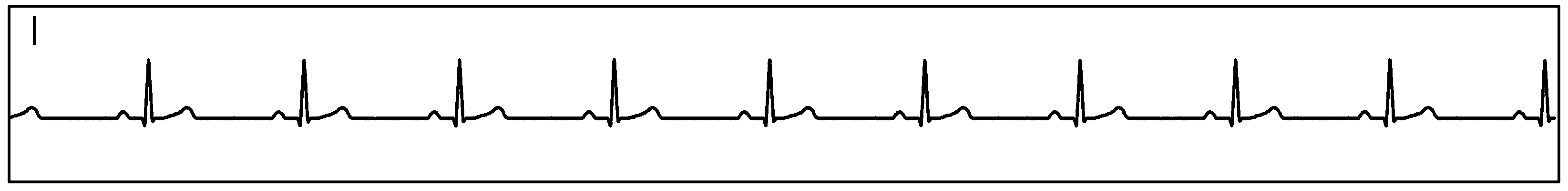
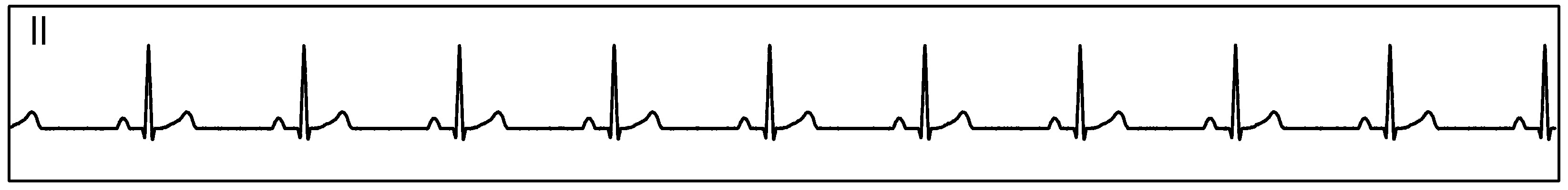
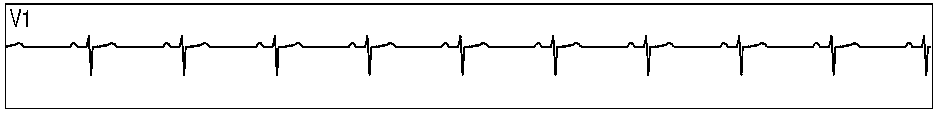
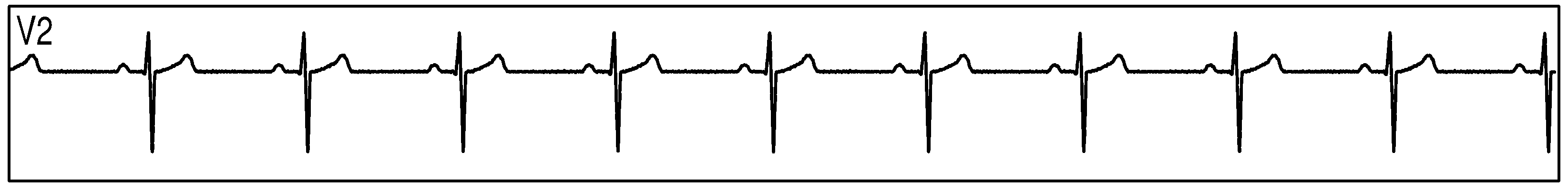
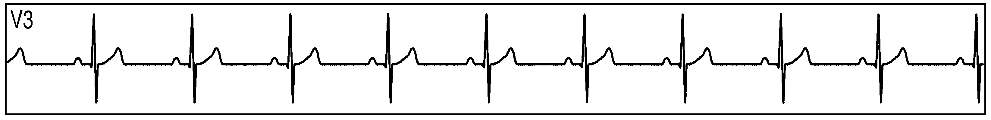
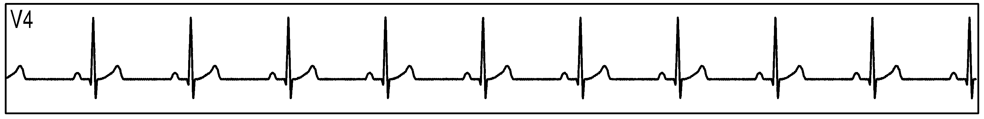
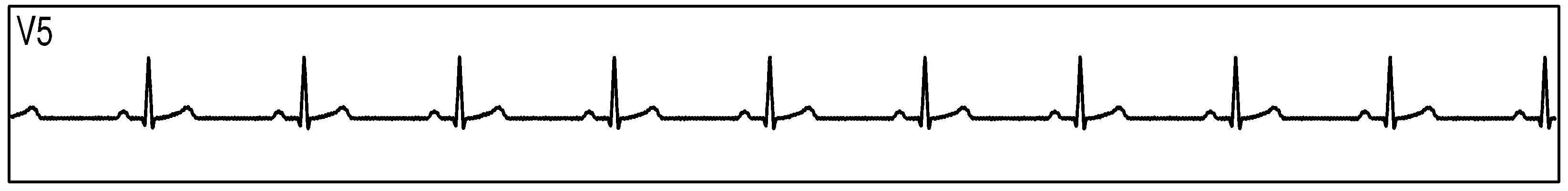
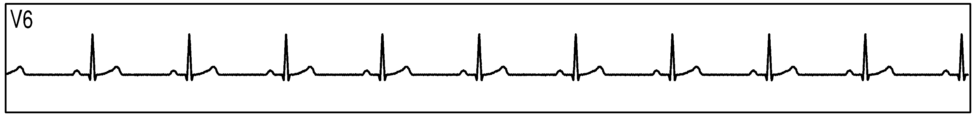 Figure 89. Three Synchornized ADS1293 Devices With an ECG Simulator: ECG Signals