SBAS459K January 2010 – August 2015 ADS1294 , ADS1294R , ADS1296 , ADS1296R , ADS1298 , ADS1298R
PRODUCTION DATA.
- 1 Features
- 2 Applications
- 3 Description
- 4 Revision History
- 5 Device Comparison
- 6 Pin Configuration and Functions
- 7 Specifications
- 8 Parameter Measurement Information
-
9 Detailed Description
- 9.1 Overview
- 9.2 Functional Block Diagram
- 9.3
Feature Description
- 9.3.1
Analog Functionality
- 9.3.1.1 EMI Filter
- 9.3.1.2 Analog Input Structure
- 9.3.1.3
Input Multiplexer
- 9.3.1.3.1 Device Noise Measurements
- 9.3.1.3.2 Test Signals (TestP and TestN)
- 9.3.1.3.3 Auxiliary Differential Input (TESTP_PACE_OUT1, TESTN_PACE_OUT2)
- 9.3.1.3.4 Temperature Sensor (TempP, TempN)
- 9.3.1.3.5 Supply Measurements (MVDDP, MVDDN)
- 9.3.1.3.6 Lead-Off Excitation Signals (LoffP, LoffN)
- 9.3.1.3.7 Auxiliary Single-Ended Input
- 9.3.1.4 Analog Input
- 9.3.1.5 PGA Settings and Input Range
- 9.3.1.6 Reference
- 9.3.1.7
ECG-Specific Functions
- 9.3.1.7.1 Input Multiplexer (Rerouting The Right Leg Drive Signal)
- 9.3.1.7.2 Input Multiplexer (Measuring The Right Leg Drive Signal)
- 9.3.1.7.3 Wilson Central Terminal (WCT) and Chest Leads
- 9.3.1.7.4 Lead-Off Detection
- 9.3.1.7.5 RLD Lead-Off
- 9.3.1.7.6 Right Leg Drive (RLD) DC Bias Circuit
- 9.3.1.7.7 Pace Detect
- 9.3.1.7.8 Respiration
- 9.3.2 Digital Functionality
- 9.3.1
Analog Functionality
- 9.4 Device Functional Modes
- 9.5
Programming
- 9.5.1 SPI Interface
- 9.5.2
SPI Command Definitions
- 9.5.2.1 WAKEUP: Exit Standby Mode
- 9.5.2.2 STANDBY: Enter Standby Mode
- 9.5.2.3 RESET: Reset Registers to Default Values
- 9.5.2.4 START: Start Conversions
- 9.5.2.5 STOP: Stop Conversions
- 9.5.2.6 RDATAC: Read Data Continuous
- 9.5.2.7 SDATAC: Stop Read Data Continuous
- 9.5.2.8 RDATA: Read Data
- 9.5.2.9 Sending Multibyte Commands
- 9.5.2.10 RREG: Read From Register
- 9.5.2.11 WREG: Write to Register
- 9.6
Register Maps
- 9.6.1
Register Descriptions
- 9.6.1.1 ID: ID Control Register (address = 00h) (reset = xxh)
- 9.6.1.2 CONFIG1: Configuration Register 1 (address = 01h) (reset = 06h)
- 9.6.1.3 CONFIG2: Configuration Register 2 (address = 02h) (reset = 40h)
- 9.6.1.4 CONFIG3: Configuration Register 3 (address = 03h) (reset = 40h)
- 9.6.1.5 LOFF: Lead-Off Control Register (address = 04h) (reset = 00h)
- 9.6.1.6 CHnSET: Individual Channel Settings (n = 1 to 8) (address = 05h to 0Ch) (reset = 00h)
- 9.6.1.7 RLD_SENSP: RLD Positive Signal Derivation Register (address = 0Dh) (reset = 00h)
- 9.6.1.8 RLD_SENSN: RLD Negative Signal Derivation Register (address = 0Eh) (reset = 00h)
- 9.6.1.9 LOFF_SENSP: Positive Signal Lead-Off Detection Register (address = 0Fh) (reset = 00h)
- 9.6.1.10 LOFF_SENSN: Negative Signal Lead-Off Detection Register (address = 10h) (reset = 00h)
- 9.6.1.11 LOFF_FLIP: Lead-Off Flip Register (address = 11h) (reset = 00h)
- 9.6.1.12 LOFF_STATP: Lead-Off Positive Signal Status Register (address = 12h) (reset = 00h)
- 9.6.1.13 LOFF_STATN: Lead-Off Negative Signal Status Register (address = 13h) (reset = 00h)
- 9.6.1.14 GPIO: General-Purpose I/O Register (address = 14h) (reset = 0Fh)
- 9.6.1.15 PACE: Pace Detect Register (address = 15h) (reset = 00h)
- 9.6.1.16 RESP: Respiration Control Register (address = 16h) (reset = 00h)
- 9.6.1.17 CONFIG4: Configuration Register 4 (address = 17h) (reset = 00h)
- 9.6.1.18 WCT1: Wilson Central Terminal and Augmented Lead Control Register (address = 18h) (reset = 00h)
- 9.6.1.19 WCT2: Wilson Central Terminal Control Register (address = 18h) (reset = 00h)
- 9.6.1
Register Descriptions
- 10Application and Implementation
- 11Power Supply Recommendations
- 12Layout
- 13Device and Documentation Support
- 14Mechanical, Packaging, and Orderable Information
Package Options
Mechanical Data (Package|Pins)
Thermal pad, mechanical data (Package|Pins)
- PAG|64
Orderable Information
7 Specifications
7.1 Absolute Maximum Ratings
over operating free-air temperature range (unless otherwise noted)(1)(1) Stresses beyond those listed under Absolute Maximum Ratings may cause permanent damage to the device. These are stress ratings only, which do not imply functional operation of the device at these or any other conditions beyond those indicated under Recommended Operating Conditions. Exposure to absolute-maximum-rated conditions for extended periods may affect device reliability.
7.2 ESD Ratings
| VALUE | UNIT | |||
|---|---|---|---|---|
| V(ESD) | Electrostatic discharge | Human body model (HBM), per ANSI/ESDA/JEDEC JS-001, all pins(1) | ±2000 | V |
| Charged device model (CDM), per JEDEC specification JESD22-C101, all pins(2) | ±500 | |||
(1) JEDEC document JEP155 states that 500-V HBM allows safe manufacturing with a standard ESD control process.
(2) JEDEC document JEP157 states that 250-V CDM allows safe manufacturing with a standard ESD control process.
7.3 Recommended Operating Conditions
over operating ambient temperature range (unless otherwise noted)| MIN | NOM | MAX | UNIT | ||
|---|---|---|---|---|---|
| POWER SUPPLY | |||||
| Analog power supply (AVDD – AVSS) | 2.7 | 3 | 5.25 | V | |
| Digital power supply (DVDD) | 1.65 | 1.8 | 3.6 | V | |
| AVDD – DVDD | –2.1 | 3.6 | V | ||
| ANALOG INPUTS | |||||
| Full-scale differential input voltage range (AINP – AINN) | ±VREF / Gain | V | |||
| Common-mode input voltage | See the Input Common-Mode Range subsection of the PGA Settings and Input Range section | ||||
| VOLTAGE REFERENCE INPUTS | |||||
| Differential reference voltage | 3-V supply VREF = (VREFP – VREFN) | 2.5 | V | ||
| 5-V supply VREF = (VREFP – VREFN) | 4 | V | |||
| Negative input (VREFN) | AVSS | V | |||
| Positive input (VREFP) | AVSS + 2.5 | V | |||
| CLOCK INPUT | |||||
| External clock input frequency | CLKSEL pin = 0 | 1.94 | 2.048 | 2.25 | MHz |
| DIGITAL INPUTS | |||||
| Input Voltage | DGND | DVDD | V | ||
| TEMPERATURE RANGE | |||||
| Operating temperature range | Commercial grade | 0 | 70 | °C | |
| Industrial grade | –40 | 85 | °C | ||
7.4 Thermal Information
| THERMAL METRIC(1) | ADS129x, ADS129xR | UNIT | ||
|---|---|---|---|---|
| PAG (TQFP) | ZXG (NFBGA) | |||
| 64 PINS | 64 PINS | |||
| RθJA | Junction-to-ambient thermal resistance | 35 | 48 | °C/W |
| RθJC(top) | Junction-to-case (top) thermal resistance | 31 | 8 | °C/W |
| RθJB | Junction-to-board thermal resistance | 26 | 25 | °C/W |
| ψJT | Junction-to-top characterization parameter | 0.1 | 0.5 | °C/W |
| ψJB | Junction-to-board characterization parameter | N/A | 22 | °C/W |
(1) For more information about traditional and new thermal metrics, see the Semiconductor and IC Package Thermal Metrics application report, SPRA953.
7.5 Electrical Characteristics
Min and max specifications apply for all commercial grade (TA = 0°C to 70°C) devices, and from TA = –40°C to +85°C for industrial-grade devices. Typical specifications at TA = 25°C. All specifications at DVDD = 1.8 V, AVDD – AVSS = 3 V(3),VREF = 2.4 V, external fCLK = 2.048 MHz, data rate = 500 SPS, HR mode(6), and gain = 6 (unless otherwise noted).
| PARAMETER | TEST CONDITIONS | MIN | TYP | MAX | UNIT | |||
|---|---|---|---|---|---|---|---|---|
| ANALOG INPUTS | ||||||||
| Input capacitance | 20 | pF | ||||||
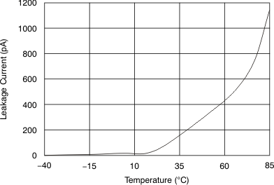
| Input bias current | TA = 25°C, input = 1.5 V | ±200 | pA | |||||
| TA = 0°C to 70°C, input = 1.5 V | ±1 | nA | ||||||
| TA = –40°C to +85°C, input = 1.5 V | ±1.2 | nA | ||||||
| DC input impedance | No lead-off | 1000 | MΩ | |||||
| Current source lead-off detection | 500 | MΩ | ||||||
| Pullup resistor lead-off detection | 10 | MΩ | ||||||
| PGA PERFORMANCE | ||||||||
| Gain settings | 1, 2, 3, 4, 6, 8, 12 | |||||||
| Bandwidth | See Table 5 | |||||||
| ADC PERFORMANCE | ||||||||
| Resolution | Data rates up to 8 kSPS, no missing codes | 24 | Bits | |||||
| 16-kSPS data rate | 19 | Bits | ||||||
| 32-kSPS data rate | 17 | Bits | ||||||
| Data rate | fCLK = 2.048 MHz, HR mode | 500 | 32000 | SPS | ||||
| fCLK = 2.048 MHz, LP mode | 250 | 16000 | SPS | |||||
| DC CHANNEL PERFORMANCE | ||||||||
| Input-referred noise | Gain = 6(1), 10 seconds of data | 5 | μVPP | |||||
| Gain = 6, 256 points, 0.5 seconds of data | 4 | 7 | μVPP | |||||
| Gain settings ≠ 6, data rates≠ 500 SPS | See Noise Measurements section | |||||||
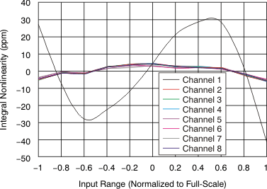
| Integral nonlinearity(5) | Full-scale with gain = 6, best fit | 8 | ppm | |||||
| Full-scale with gain = 6, best fit, ADS129xR channel 1 |
40 | ppm | ||||||
| –20 dBFS with gain = 6, best fit, ADS129xR channel 1 |
8 | ppm | ||||||
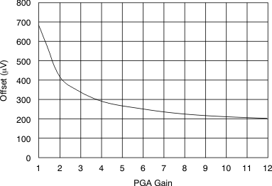
| Offset error | ±500 | µV | ||||||
| Offset error drift | 2 | µV/°C | ||||||
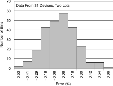
| Gain error | Excluding voltage reference error | ±0.2 | ±0.5 | % of FS | ||||
| Gain drift | Excluding voltage reference drift | 5 | ppm/°C | |||||
| Gain match between channels | 0.3 | % of FS | ||||||
| AC CHANNEL PERFORMANCE | ||||||||
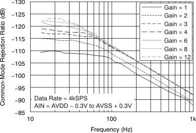
| CMRR | Common-mode rejection ratio | fCM = 50 Hz, 60 Hz(2) | –105 | –115 | dB | |||
| PSRR | Power-supply rejection ratio | fPS = 50 Hz, 60 Hz | 90 | dB | ||||
| Crosstalk | fIN = 50 Hz, 60 Hz | –126 | dB | |||||
| SNR | Signal-to-noise ratio | fIN = 10 Hz input, gain = 6 | 112 | dB | ||||
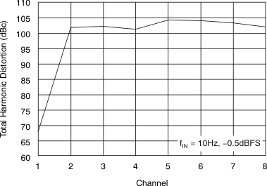
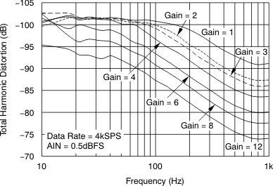
| THD | Total harmonic distortion(5) | 10 Hz, –0.5 dBFs | –98 | dB | ||||
| ADS129xR channel 1, 10 Hz, –0.5 dBFs | –70 | dB | ||||||
| 100 Hz, –0.5 dBFs(4) | –100 | dB | ||||||
| ADS129xR channel 1, 100 Hz, –0.5 dBFs(4) | –68 | dB | ||||||
| ADS129xR channel 1, 100 Hz, –20 dBFs(4) | –86 | dB | ||||||
| DIGITAL FILTER | ||||||||
| –3-dB bandwidth | 0.262 fDR | Hz | ||||||
| Digital filter settling | Full setting | 4 | Conversions | |||||
| RIGHT LEG DRIVE (RLD) AMPLIFIER AND PACE AMPLIFIERS | ||||||||
| RLD integrated noise | BW = 150 Hz | 7 | μVRMS | |||||
| Pace integrated noise | BW = 8 kHz | 20 | µVRMS | |||||
| Pace-amplifier crosstalk | Crosstalk between pace amplifiers | 60 | dB | |||||
| Gain bandwidth product | 50 kΩ || 10 pF load, gain = 1 | 100 | kHz | |||||
| Slew rate | 50 kΩ || 10 pF load, gain = 1 | 0.25 | V/μs | |||||
| Pace and RLD amplifier drive strength | Short circuit to GND (AVDD = 3 V) | 270 | μA | |||||
| Short circuit to supply (AVDD = 3 V) | 550 | μA | ||||||
| Short circuit to GND (AVDD = 5 V) | 490 | μA | ||||||
| Short circuit to supply (AVDD = 5 V) | 810 | μA | ||||||
| Pace and RLD current | Peak swing (AVSS + 0.3 V to AVDD + 0.3 V) at AVDD = 3 V |
50 | μA | |||||
| Peak swing (AVSS + 0.3 V to AVDD + 0.3 V) at AVDD = 5 V |
75 | μA | ||||||
| Pace-amplifier output resistance | 100 | Ω | ||||||
| Total harmonic distortion | fIN = 100 Hz, gain = 1 | –70 | dB | |||||
| Common-mode input range | AVSS + 0.7 | AVDD – 0.3 | V | |||||
| Common-mode resistor matching | Internal 200-kΩ resistor matching | 0.1% | ||||||
| Short-circuit current | ±0.25 | mA | ||||||
| Quiescent power consumption | Either RLD or pace amplifier | 20 | μA | |||||
| WILSON CENTRAL TERMINAL (WCT) AMPLIFIER | ||||||||
| Integrated noise | BW = 150 Hz | See Table 6 | nV/√Hz | |||||
| Gain bandwidth product | See Table 6 | kHz | ||||||
| Slew rate | See Table 6 | V/s | ||||||
| Total harmonic distortion | fIN = 100 Hz | 90 | dB | |||||
| Common-mode input range | AVSS + 0.3 | AVDD – 0.3 | V | |||||
| Short-circuit current | Through internal 30-kΩ resistor | ±0.25 | mA | |||||
| Quiescent power consumption | See Table 6 | μA | ||||||
| LEAD-OFF DETECT | ||||||||
| Frequency | See Table 16 for settings | 0, fDR/4 | kHz | |||||
| Current | See Table 16 for settings | 6, 12, 18, 24 | nA | |||||
| Current accuracy | ±20% | |||||||
| Comparator threshold accuracy | ±30 | mV | ||||||
| RESPIRATION (ADS129xR ONLY) | ||||||||
| Frequency | Internal source | 32, 64 | kHz | |||||
| External source | 32 | 64 | kHz | |||||
| Phase shift | See Table 16 for settings | 22.5 | 90 | 157.5 | Degrees | |||
| Impedance range | IRESP = 30 μA | 10 | kΩ | |||||
| Impedance measurement noise | 0.05-Hz to 2-Hz brick wall filter, 32-kHz modulation clock, phase = 112.5, IRESP = 30 μA with 2-kΩ baseline load, gain = 4 | 20 | mΩPP | |||||
| Modulator current | internal reference, signal path = 82 kΩ, baseline = 2.21 kΩ |
29 | µA | |||||
| EXTERNAL REFERENCE | ||||||||
| Input impedance | 10 | kΩ | ||||||
| INTERNAL REFERENCE | ||||||||
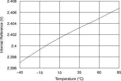
| Output voltage | Register bit CONFIG3.VREF_4V = 0, AVDD ≥ 2.7 V |
2.4 | V | |||||
| Register bit CONFIG3.VREF_4V = 1, AVDD ≥ 4.4 V |
4 | V | ||||||
| VREF accuracy | ±0.2% | |||||||
| Internal reference drift | TA = 25°C | 35 | ppm/°C | |||||
| Commercial grade, 0°C to 70°C | 35 | ppm | ||||||
| Industrial grade, –40°C to 85°C | 45 | ppm | ||||||
| Start-up time | 150 | ms | ||||||
| SYSTEM MONITORS | ||||||||
| Analog-supply reading error | 2% | |||||||
| Digital-supply reading error | 2% | |||||||
| Device wakeup | From power up to DRDY low | 150 | ms | |||||
| STANDBY mode | 9 | ms | ||||||
| Temperature-sensor reading, voltage | TA = 25°C | 145 | mV | |||||
| Temperature-sensor reading, coefficient | 490 | μV/°C | ||||||
| Test-signal frequency | See Table 16 for settings | fCLK / 221, fCLK / 220 | Hz | |||||
| Test-signal voltage | See Table 16 for settings | ±1, ±2 | mV | |||||
| Test-signal accuracy | ±2% | |||||||
| CLOCK | ||||||||
| Internal-oscillator clock frequency | Nominal frequency | 2.048 | MHz | |||||
| Internal clock accuracy | TA = 25°C | ±0.5% | ||||||
| 0°C ≤ TA ≤ 70°C | ±2% | |||||||
| –40°C ≤ TA ≤ 85°C, industrial grade versions only | ±2.5% | |||||||
| Internal-oscillator start-up time | 20 | μs | ||||||
| Internal-oscillator power consumption | 120 | μW | ||||||
| DIGITAL INPUT/OUTPUT (DVDD = 1.65 V to 3.6 V) | ||||||||
| VIH | High-level inpout voltage | 0.8 DVDD | DVDD + 0.1 | V | ||||
| VIL | Low-level input voltage | –0.1 | 0.2 DVDD | V | ||||
| VOH | High-level output voltage | IOH = –500 μA | DVDD – 0.4 | V | ||||
| VOL | Low-level output voltage | IOL = 500 μA | 0.4 | V | ||||
| IIN | Input current | 0 V < VDigitalInput < DVDD | –10 | 10 | μA | |||
| POWER SUPPLY (RLD, WCT, AND PACE AMPLIFIERS TURNED OFF) | ||||||||
| IAVDD | AVDD current | AVDD – AVSS = 3 V | HR mode (ADS1298) | 2.75 | mA | |||
| LP mode(6) (ADS1298) | 1.8 | mA | ||||||
| AVDD – AVSS = 5 V | HR mode (ADS1298) | 3.1 | mA | |||||
| LP mode (ADS1298) | 2.1 | mA | ||||||
| IDVDD | DVDD current | DVDD = 1.8 V | HR mode (ADS1298) | 0.3 | mA | |||
| LP mode (ADS1298) | 0.3 | mA | ||||||
| DVDD = 3 V | HR mode (ADS1298) | 0.5 | mA | |||||
| LP mode (ADS1298) | 0.5 | mA | ||||||
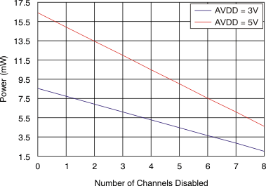
| Power dissipation | ADS1298, ADS1298R, AVDD – AVSS = 3 V | HR mode | 8.8 | 9.5 | mW | |||
| LP mode (250 SPS) | 6.0 | 7.0 | mW | |||||
| ADS1296, ADS1296R, AVDD – AVSS = 3 V | HR mode | 7.2 | 7.9 | mW | ||||
| LP mode (250 SPS) | 5.3 | 6.6 | mW | |||||
| ADS1294, ADS1294R, AVDD – AVSS = 3 V | HR mode | 5.4 | 6 | mW | ||||
| LP mode (250 SPS) | 4.1 | 4.4 | mW | |||||
| ADS1298, ADS1298R, AVDD – AVSS = 5 V | HR mode | 17.5 | mW | |||||
| LP mode (250 SPS) | 12.5 | mW | ||||||
| ADS1296, ADS1296R, AVDD – AVSS = 5 V | HR mode | 14.1 | mW | |||||
| LP mode (250 SPS) | 10 | mW | ||||||
| ADS1294, ADS1294R, AVDD – AVSS = 5 V | HR mode | 10.1 | mW | |||||
| LP mode (250 SPS) | 8.3 | mW | ||||||
| Power-down | AVDD – AVSS = 3 V | 10 | μW | |||||
| AVDD – AVSS = 5 V | 20 | μW | ||||||
| Standby mode | AVDD – AVSS = 3 V | 2 | mW | |||||
| AVDD – AVSS = 5 V | 4 | mW | ||||||
| Quiescent channel power | AVDD – AVSS = 3 V, PGA + ADC | 818 | μW | |||||
| AVDD – AVSS = 5 V, PGA + ADC | 1.5 | mW | ||||||
(1) Noise data measured in a 10-second interval. Test not performed in production. Input-referred noise is calculated with input shorted (without electrode resistance) over a 10-second interval.
(2) CMRR is measured with a common-mode signal of AVSS + 0.3 V to AVDD – 0.3 V. The values indicated are the maximum of the eight channels.
(3) Performance is applicable for 5-V operation as well. Production testing for limits is performed at 3 V.
(4) Harmonics above the second harmonic are attenuated by the digital filter.
(5) The presence of internal demodulation circuitry on channel 1 causes degradation of INL and THD. The effect is pronounced for full-scale signals and is less for small ECG-type signals.
(6) LP mode = low-power mode.
7.6 Timing Requirements: Serial Interface
specifications apply from TA = –40°C to +85°C (unless otherwise noted); load on DOUT = 20 pF || 100 kΩ| 2.7 V ≤ DVDD ≤ 3.6 V | 1.65 V ≤ DVDD ≤ 2 V | UNIT | ||||
|---|---|---|---|---|---|---|
| MIN | MAX | MIN | MAX | |||
| tCLK | Master clock period | 414 | 514 | 414 | 514 | ns |
| tCSSC | CS low to first SCLK, setup time | 6 | 17 | ns | ||
| tSCLK | SCLK period | 50 | 66.6 | ns | ||
| tSPWH, L | SCLK pulse width, high and low | 15 | 25 | ns | ||
| tDIST | DIN valid to SCLK falling edge: setup time | 10 | 10 | ns | ||
| tDIHD | Valid DIN after SCLK falling edge: hold time | 10 | 11 | ns | ||
| tCSH | CS high pulse | 2 | 2 | tCLK | ||
| tSCCS | Eighth SCLK falling edge to CS high | 4 | 4 | tCLK | ||
| tSDECODE | Command decode time | 4 | 4 | tCLK | ||
| tDISCK2ST | DAISY_IN valid to SCLK rising edge: setup time | 10 | 10 | ns | ||
| tDISCK2HT | DAISY_IN valid after SCLK rising edge: hold time | 10 | 10 | ns | ||
7.7 Switching Characteristics: Serial Interface
specifications apply from TA = –40°C to +85°C (unless otherwise noted). Load on DOUT = 20 pF || 100 kΩ.| PARAMETER | 2.7 V ≤ DVDD ≤ 3.6 V | 1.65 V ≤ DVDD ≤ 2 V | UNIT | |||
|---|---|---|---|---|---|---|
| MIN | MAX | MIN | MAX | |||
| tDOHD | SCLK falling edge to invalid DOUT: hold time | 10 | 10 | ns | ||
| tDOPD | SCLK rising edge to DOUT valid: setup time | 17 | 32 | ns | ||
| tCSDOD | CS low to DOUT driven | 10 | 20 | ns | ||
| tCSDOZ | CS high to DOUT Hi-Z | 10 | 20 | ns | ||
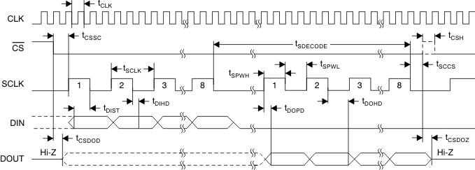
NOTE: SPI settings are CPOL = 0 and CPHA = 1.
Figure 1. Serial Interface Timing

NOTE: Daisy-chain timing shown for eight-channel ADS1298 and ADS1298R.
Figure 2. Daisy-Chain Interface Timing
7.8 Typical Characteristics
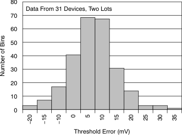
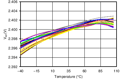
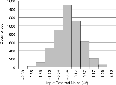
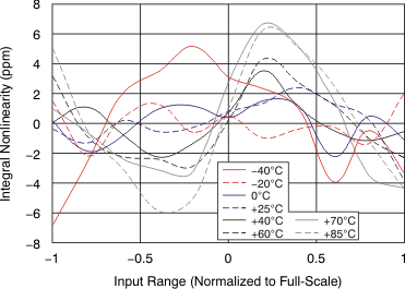
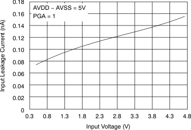
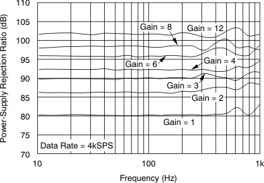
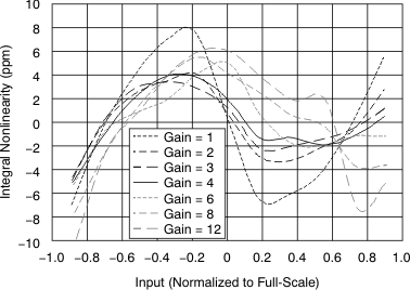
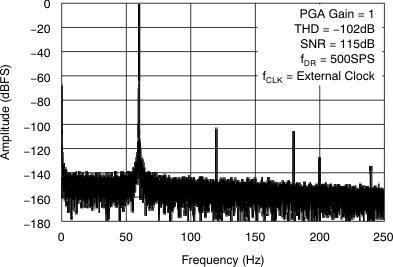
at TA = 25°C, AVDD = 3 V, AVSS = 0 V, DVDD = 1.8 V, internal VREFP = 2.4 V, VREFN = AVSS, external clock = 2.048 MHz, data rate = 500 SPS, high-resolution mode, and gain = 6 (unless otherwise noted)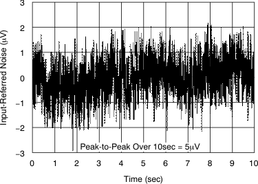
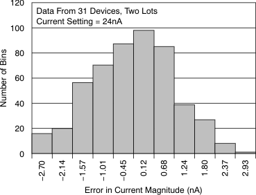
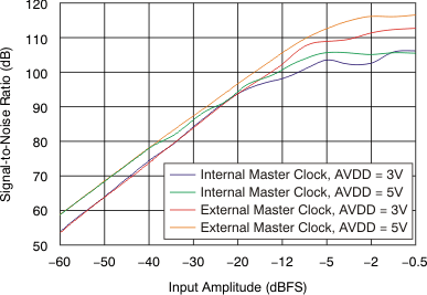
(10-Hz Sine Wave)
