SBAS578A May 2012 – January 2016 ADS4128
PRODUCTION DATA.
- 1 Features
- 2 Applications
- 3 Description
- 4 Revision History
- 5 Device Comparison Table
- 6 Pin Configuration and Functions
-
7 Specifications
- 7.1 Absolute Maximum Ratings
- 7.2 ESD Ratings
- 7.3 Recommended Operating Conditions
- 7.4 Thermal Information
- 7.5 Electrical Characteristics
- 7.6 Electrical Characteristics: General
- 7.7 Digital Characteristics
- 7.8 Timing Requirements: LVDS and CMOS Modes
- 7.9 Reset Timing Requirements
- 7.10 Typical Characteristics
- 7.11 Typical Characteristics: Contour
-
8 Detailed Description
- 8.1 Overview
- 8.2 Functional Block Diagram
- 8.3 Feature Description
- 8.4 Device Functional Modes
- 8.5 Programming
- 8.6 Register Maps
- 9 Application and Implementation
- 10Power Supply Recommendations
- 11Layout
- 12Device and Documentation Support
- 13Mechanical, Packaging, and Orderable Information
Package Options
Mechanical Data (Package|Pins)
- RGZ|48
Thermal pad, mechanical data (Package|Pins)
- RGZ|48
Orderable Information
1 Features
- Maximum Sample Rate: 200 MSPS
- Ultralow Power with 1.8-V Single Supply:
- 230-mW Total Power at 200 MSPS
- High Dynamic Performance:
- SNR: 69 dBFS at 170 MHz
- SFDR: 85 dBc at 170 MHz
- Dynamic Power Scaling With Sample Rate
- Output Interface:
- Double Data Rate (DDR) LVDS with Programmable Swing and Strength
- Standard Swing: 350 mV
- Low Swing: 200 mV
- Default Strength: 100-Ω Termination
- 2× Strength: 50-Ω Termination
- 1.8-V Parallel CMOS Interface Also Supported
- Double Data Rate (DDR) LVDS with Programmable Swing and Strength
- Programmable Gain up to 6 dB for SNR and SFDR Trade-Off
- DC Offset Correction
- Supports Low Input Clock Amplitude Down to 200 mVPP
- Package: 7.00 mm × 7.00 mm VQFN-48
2 Applications
- Wireless Communications Infrastructure
- Software-Defined Radio
- Power Amplifier Linearization
3 Description
The ADS4128 is a 12-bit analog-to-digital converter (ADC) with sampling rates up to 200 MSPS. This device uses innovative design techniques to achieve high dynamic performance, while consuming extremely low power at 1.8-V supply. The device is well-suited for multi-carrier, wide-bandwidth communications applications.
The ADS4128 has fine-gain options that can be used to improve SFDR performance at lower full-scale input ranges, especially at high input frequencies. It includes a dc offset correction loop that can be used to cancel the ADC offset. At lower sampling rates, the ADC automatically operates at scaled-down power with no loss in performance.
The ADS4128 is available in a compact VQFN-48 package and is specified over the industrial temperature range (–40°C to 85°C).
Device Information(1)
| PART NUMBER | PACKAGE | BODY SIZE (NOM) |
|---|---|---|
| ADS4128 | VQFN(48) | 7.00 mm × 7.00 mm |
- For all available packages, see the orderable addendum at the end of the data sheet.
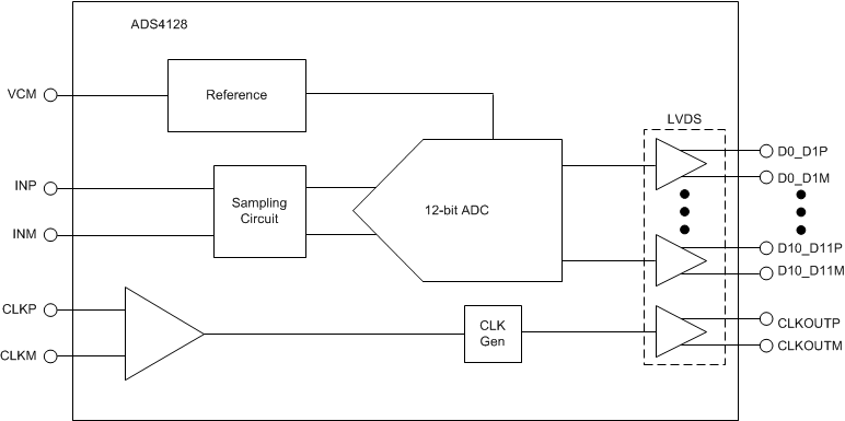
ADS4128 Block Diagram
