SLAS900F October 2012 – December 2014 ADS42JB49 , ADS42JB69
PRODUCTION DATA.
- 1 Features
- 2 Applications
- 3 Description
- 4 Revision History
- 5 Device Comparison Table
- 6 Pin Configuration and Functions
-
7 Specifications
- 7.1 Absolute Maximum Ratings
- 7.2 ESD Ratings
- 7.3 Recommended Operating Conditions
- 7.4 Thermal Information
- 7.5 Electrical Characteristics: ADS42JB69 (16-Bit)
- 7.6 Electrical Characteristics: ADS42JB49 (14-Bit)
- 7.7 Electrical Characteristics: General
- 7.8 Digital Characteristics
- 7.9 Timing Characteristics
- 7.10 Typical Characteristics: ADS42JB69
- 7.11 Typical Characteristics: ADS42JB49
- 7.12 Typical Characteristics: Common
- 7.13 Typical Characteristics: Contour
- 8 Parameter Measurement Information
-
9 Detailed Description
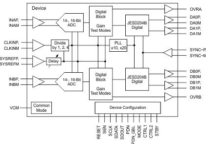
- 9.1 Overview
- 9.2 Functional Block Diagram
- 9.3 Feature Description
- 9.4 Device Functional Modes
- 9.5 Programming
- 9.6
Register Maps
- 9.6.1
Description of Serial Interface Registers
- 9.6.1.1 Register 6 (offset = 06h) [reset = 00h]
- 9.6.1.2 Register 7 (offset = 07h) [reset = 00h]
- 9.6.1.3 Register 8 (offset = 08h) [reset = 00h]
- 9.6.1.4 Register B (offset = 0Bh) [reset = 00h]
- 9.6.1.5 Register C (offset = 0Ch) [reset = 00h]
- 9.6.1.6 Register D (offset = 0Dh) [reset = 00h]
- 9.6.1.7 Register E (offset = 0Eh) [reset = 00h]
- 9.6.1.8 Register F (offset = 0Fh) [reset = 00h]
- 9.6.1.9 Register 10 (offset = 10h) [reset = 00h]
- 9.6.1.10 Register 11 (offset = 11h) [reset = 00h]
- 9.6.1.11 Register 12 (offset = 12h) [reset = 00h]
- 9.6.1.12 Register 13 (offset = 13h) [reset = 00h]
- 9.6.1.13 Register 1F (offset = 1Fh) [reset = FFh]
- 9.6.1.14 Register 26 (offset = 26h) [reset = 00h]
- 9.6.1.15 Register 27 (offset = 27h) [reset = 00h]
- 9.6.1.16 Register 2B (offset = 2Bh) [reset = 00h]
- 9.6.1.17 Register 2C (offset = 2Ch) [reset = 00h]
- 9.6.1.18 Register 2D (offset = 2Dh) [reset = 00h]
- 9.6.1.19 Register 30 (offset = 30h) [reset = 40h]
- 9.6.1.20 Register 36 (offset = 36h) [reset = 00h]
- 9.6.1.21 Register 37 (offset = 37h) [reset = 00h]
- 9.6.1.22 Register 38 (offset = 38h) [reset = 00h]
- 9.6.1
Description of Serial Interface Registers
- 10Application and Implementation
- 11Power Supply Recommendations
- 12Layout
- 13Device and Documentation Support
- 14Mechanical, Packaging, and Orderable Information
Package Options
Mechanical Data (Package|Pins)
- RGC|64
Thermal pad, mechanical data (Package|Pins)
- RGC|64
Orderable Information
1 Features
- Dual-Channel ADCs
- 14- and 16-Bit Resolution
- Maximum Clock Rate: 250 MSPS
- JESD204B Serial Interface
- Subclass 0, 1, 2 Compliant
- Up to 3.125 Gbps
- Two and Four Lanes Support
- Analog Input Buffer with High-Impedance Input
- Flexible Input Clock Buffer:
Divide-by-1, -2, and -4 - Differential Full-Scale Input: 2 VPP and 2.5 VPP
(Register Programmable) - Package: 9-mm × 9-mm VQFN-64
- Power Dissipation: 850 mW/Ch
- Aperture Jitter: 85 fS rms
- Internal Dither
- Channel Isolation: 100 dB
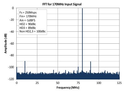
- Performance:
- fIN = 170 MHz at 2 VPP, –1 dBFS
- SNR: 73.3 dBFS
- SFDR: 93 dBc for HD2, HD3
- SFDR: 100 dBc for Non HD2, HD3
- fIN = 170 MHz at 2.5 VPP, –1 dBFS
- SNR: 74.7 dBFS
- SFDR: 89 dBc for HD2, HD3 and
95 dBc for Non HD2, HD3
- fIN = 170 MHz at 2 VPP, –1 dBFS
2 Applications
- Communication and Cable Infrastructure
- Multi-Carrier, Multimode Cellular Receivers
- Radar and Smart Antenna Arrays
- Broadband Wireless
- Test and Measurement Systems
- Software-Defined and Diversity Radios
- Microwave and Dual-Channel I/Q Receivers
- Repeaters
- Power Amplifier Linearization
3 Description
The ADS42JB69 and ADS42JB49 are high-linearity, dual-channel, 16- and 14-bit, 250-MSPS, analog-to-digital converters (ADCs). These devices support the JESD204B serial interface with data rates up to
3.125 Gbps. The buffered analog input provides uniform input impedance across a wide frequency range while minimizing sample-and-hold glitch energy making it easy to drive analog inputs up to very high input frequencies. A sampling clock divider allows more flexibility for system clock architecture design. The devices employ internal dither algorithms to provide excellent spurious-free dynamic range (SFDR) over a large input frequency range.
Device Information(1)
| PART NUMBER | PACKAGE | INTERFACE OPTION |
|---|---|---|
| ADS42JB49 | VQFN (64) | 14-bit DDR or QDR LVDS |
| 14-bit JESD204B | ||
| ADS42JB69 | VQFN (64) | 16-bit DDR or QDR LVDS |
| 16-bit JESD204B |
- For all available packages, see the orderable addendum at the end of the datasheet.