SBAS773A September 2017 – December 2017 ADS7142
PRODUCTION DATA.
- 1 Features
- 2 Applications
- 3 Description
- 4 Revision History
- 5 Pin Configuration and Functions
-
6 Specifications
- 6.1 Absolute Maximum Ratings
- 6.2 ESD Ratings
- 6.3 Recommended Operating Conditions
- 6.4 Thermal Information
- 6.5 Electrical Characteristics - All Modes
- 6.6 Electrical Characteristics - Manual Mode
- 6.7 Electrical Characteristics - Autonomous Modes
- 6.8 Electrical Characteristics - High Precision Mode
- 6.9 Timing Requirements
- 6.10 Switching Characteristics
- 6.11 Typical Characteristics for All Modes
- 6.12 Typical Characteristics for Manual Mode
- 6.13 Typical Characteristics for Autonomous Modes
- 6.14 Typical Characteristics for High Precision Mode
-
7 Detailed Description
- 7.1 Overview
- 7.2 Functional Block Diagram
- 7.3 Feature Description
- 7.4 Device Functional Modes
- 7.5 Optimizing Power Consumed by the Device
- 7.6
Register Map
- 7.6.1 RESET REGISTERS
- 7.6.2 FUNCTIONAL MODE SELECT REGISTERS
- 7.6.3 INPUT CONFIG REGISTER
- 7.6.4 ANALOG MUX and SEQUENCER REGISTERS
- 7.6.5 OSCILLATOR and TIMING CONTROL REGISTERS
- 7.6.6 DATA BUFFER CONTROL REGISTER
- 7.6.7
ACCUMULATOR CONTROL REGISTERS
- 7.6.7.1 ACC_EN Register (address = 30h), [reset = 00h]
- 7.6.7.2 ACC_CH0_LSB Register (address = 08h), [reset = 00h]
- 7.6.7.3 ACC_CH0_MSB Register (address = 09h), [reset = 00h]
- 7.6.7.4 ACC_CH1_LSB Register (address = 0Ah), [reset = 00h]
- 7.6.7.5 ACC_CH1_MSB Register (address = 0Bh), [reset = 00h]
- 7.6.7.6 ACCUMULATOR_STATUS Register (address = 02h), [reset = 00h]
- 7.6.8
DIGITAL WINDOW COMPARATOR REGISTERS
- 7.6.8.1 ALERT_DWC_EN Register (address = 37h), [reset = 00h]
- 7.6.8.2 ALERT_CHEN (address = 34h), [reset = 00h]
- 7.6.8.3 DWC_HTH_CH0_MSB Register (address = 39h), [reset = 00h]
- 7.6.8.4 DWC_HTH_CH0_LSB Register (address = 38h), [reset = 00h]
- 7.6.8.5 DWC_LTH_CH0_MSB Register (address = 3Bh), [reset = 00h]
- 7.6.8.6 DWC_LTH_CH0_LSB Register (address = 3Ah), [reset = 00h]
- 7.6.8.7 DWC_HYS_CH0 (address = 40h), [reset = 00h]
- 7.6.8.8 DWC_HTH_CH1_MSB Register (address = 3Dh), [reset = 00h]
- 7.6.8.9 DWC_HTH_CH1_LSB Register (address = 3Ch), [reset = 00h]
- 7.6.8.10 DWC_LTH_CH1_MSB Register (address = 3Fh), [reset = 00h]
- 7.6.8.11 DWC_LTH_CH1_LSB Register (address = 3Eh), [reset = 00h]
- 7.6.8.12 DWC_HYS_CH1 (address = 41h), [reset = 00h]
- 7.6.8.13 PRE_ALT_MAX_EVENT_COUNT Register (address = 36h), [reset = 00h]
- 7.6.8.14 ALERT_TRIG_CHID Register (address = 03h), [reset = 00h]
- 7.6.8.15 ALERT_LOW_FLAGS Register (address = 0C), [reset = 00h]
- 7.6.8.16 ALERT_HIGH_FLAGS Register (address = 0Eh), [reset = 00h]
- 8 Application and Implementation
- 9 Power-Supply Recommendations
- 10Layout
- 11Device and Documentation Support
- 12Mechanical, Packaging, and Orderable Information
Package Options
Mechanical Data (Package|Pins)
- RUG|10
Thermal pad, mechanical data (Package|Pins)
Orderable Information
8 Application and Implementation
NOTE
Information in the following applications sections is not part of the TI component specification, and TI does not warrant its accuracy or completeness. TI’s customers are responsible for determining suitability of components for their purposes. Customers should validate and test their design implementation to confirm system functionality.
8.1 Application Information
In an increasing number of industrial applications, data acquisition sub-systems are collecting more data about the environment in which the system is operating and applying deep learning algorithms in order to improve system reliability, implement preventative maintenance, and/or enhance the quality of data collected by the system. The ADS7142 can be used to connect to a variety of sensors and can provide deeper data analytics at lower power levels than existing solutions. The depth of analysis that can be performed on the data collected by the ADS7142 is enhanced by the internal data buffer, programmable alarm thresholds and hysteresis, event counter, and internal calibration circuitry. The applications circuits described in this section highlight specific use-cases of the ADS7142 for data collection that can further increase the depth and quality of the data being measured by the system.
8.2 Typical Applications
8.2.1 ADS7142 as a Programmable Comparator with False Trigger Prevention and Diagnostics
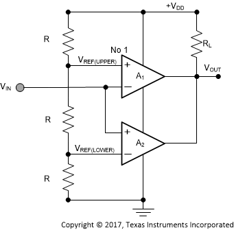 Figure 112. Analog Window Comparator
8.2.1.1 Design Requirements
In many applications such as industrial alarms, sensor monitors, and level sensors, there is a need to make a decision at the system-level when the input signal crosses a predefined threshold. Analog window comparators are being used extensively in such applications.
An analog window comparator has a set of comparators. The external input signal is connected to the inverting terminal of one comparator and the noninverting terminal of the other comparator. The remaining input of each comparator is connected to the internal reference. The outputs are tied together and are often connected to a reset or general-purpose input of a processor (such as a digital signal processor, field-programmable gate array, or application-specific integrated circuit) or the enable input of a voltage regulator (such as a DC-DC or low-dropout regulator). Figure 112 shows the circuit diagram for an analog window comparator.
Though analog comparators are easy to design, there are certain disadvantages associated with analog comparators.
8.2.1.1.1 Higher Power Consumption
If the voltage that is monitored is greater than the window comparator supply voltage, then there is a need for a resistive divider ladder to scale down that voltage. This resistive ladder draws a constant current and adds to the power consumption of the system. In battery powered applications, this becomes a challenge and can adversely affect the battery life.
8.2.1.1.2 Fixed Threshold Voltages
The window comparator thresholds cannot be changed on-the-fly since these are set by hardware (typically with a resistive ladder). This may add a limitation if the user wants to change the comparator thresholds during operation without switching in a new resistor ladder.
Many applications in the field of preventive maintenance, building automation, and Internet of Things (IoT) require a sensor monitor which operates autonomously and gives an alert/interrupt to the host MCU only when the sensor output crosses a predefined, programmable threshold. Typically battery-operated, wireless sensor nodes like smoke detectors, temperature monitors, ambient light sensors, proximity sensors and gas sensors fall under this category. The ADS7142 is an excellent fit for such sensor monitoring systems due to its ability to autonomously monitor sensor output and wake up the host controller whenever the sensor output crosses pre-defined thresholds. Additionally, the ADS7142 has an internal data buffer which can store 16 sample data which the user can read if further analysis is required. Figure 113 shows typical block diagram of ADS7142 as sensor monitor. As is shown in Figure 113, the sensor can be connected directly to the input of the ADC (depending on the sensor output signal characteristics).
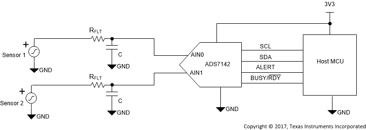 Figure 113. Sensor Monitor Circuit with ADS7142
8.2.1.2 Detailed Design Procedure
8.2.1.2.1 Programmable Thresholds and Hysteresis
The ADS7142 can be programmed to monitor sensor output voltages and generate an ALERT signal for the host controller if the sensor output voltage crosses a threshold.
The device can be configured to monitor for signals rising above a programmed threshold. Figure 114 illustrates the operation of the device when monitoring for signal crossings on the low threshold by setting the high threshold to 0xFFF. In this example, the output of the low-side comparator is set whenever the ADC conversion result is less than or equal to the low threshold, and the output of the high-side comparator is only set when the ADC conversion result is equal to 0xFFF.
The device can also be configured to monitor for signals falling below a programmed threshold. Figure 115 illustrates the operation of the device when monitoring for signal crossings on the high threshold by setting the low threshold to 0x000. In this example, the output of high-side comparator is set whenever the ADC conversion result is greater than or equal to the high threshold and the output of the low-side comparator is only set when the ADC conversion result is equal to 0x000.
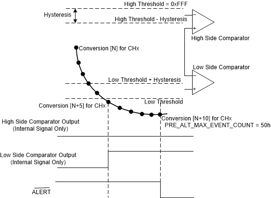 Figure 114. Low Alert with ADS7142
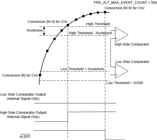 Figure 115. High Alert with ADS7142
The device can also be configured to monitor for signals falling outside of a programmed window. Figure 116 illustrates the operation of the device for an out-of-range alert where the signal leaves the pre-defined window and crosses either the high or low threshold. In this example, the output of low side comparator is set whenever the ADC conversion result is less than or equal to the low threshold, and the output of high side comparator is set when the ADC conversion result is greater than or equal to the high threshold.
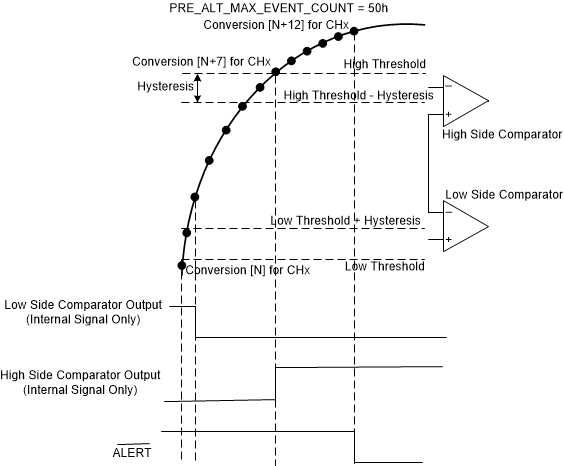 Figure 116. Out of Range Alert with ADS7142
8.2.1.2.2 False Trigger Prevention with Event Counter
The Pre-Alert event counter in the Digital Window Comparator helps to prevent false triggers. The alert output is not set until the output of the comparator remains set for a pre-defined number (count) of consecutive conversions.
8.2.1.2.3 Fault Diagnostics with Data Buffer
The modes which are specifically designed for autonomous sensor monitor applications are Pre-Alert mode and Post-Alert mode. In Pre-Alert mode, the ADS7142 can be configured to monitor sensor outputs and continuously fill the internal data buffer until a threshold crossing occurs. The ADS7142 generates an ALERT signal when the sensor output falls outside of the predefined window of operation. In this particular mode, the ADS7142 stops filling the data buffer when the threshold is crossed and provides the last 16 samples (15 sample data preceding the sample at which the ALERT is generated and 1 sample data for which the ALERT is generated). Figure 117 shows the ADS7142 operation in Pre-Alert mode showing 16 data samples before the sensor output crosses the low threshold. This is useful for applications where the state of the signal before the threshold is crossed is important to capture. Using the data captured before the alert, deep data analysis can be performed to determine the state of the system before the alert. This type of data is not available with analog comparators.
In Post-Alert mode, ADS7142 can be configured to monitor sensor outputs and start filling the internal data buffer after a threshold crossing occurs. The ADS7142 generates an ALERT signal when the sensor output falls outside of the predefined window of operation. In this particular mode, the ADS7142 continues to fill the data buffer after the threshold is crossed for a total of 16 samples (1 sample data for which ALERT is generated and 15 sample data after the sample at which ALERT is generated). Figure 118 shows the ADS7142 operation in Post-Alert mode showing 16 data samples after the sensor output crosses the high threshold. This is useful for applications where the state of the signal after the threshold is crossed is important to capture. Using the data captured after the alert, deep data analysis can be performed for to determine the state of the system after the alert to detect system-level events such as saturation. This data is not available with analog comparators.
8.2.1.3 Application Curve
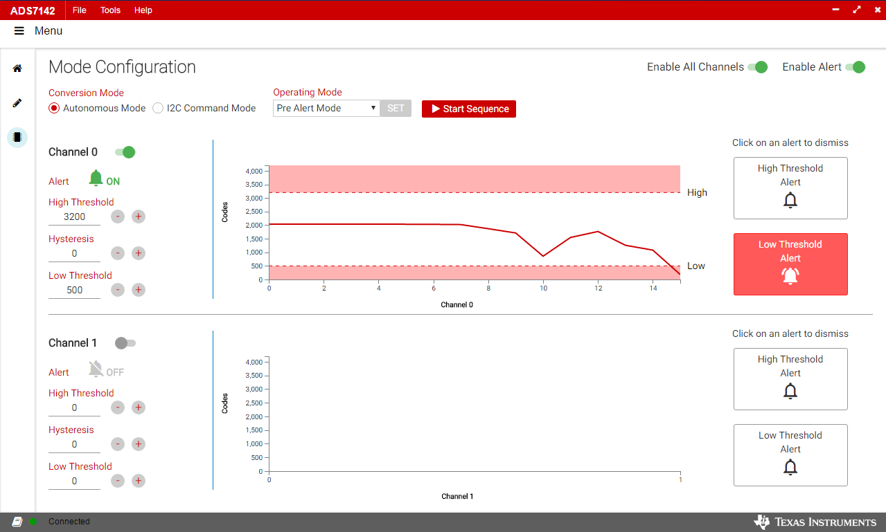 Figure 117. Pre-Alert Data Capture
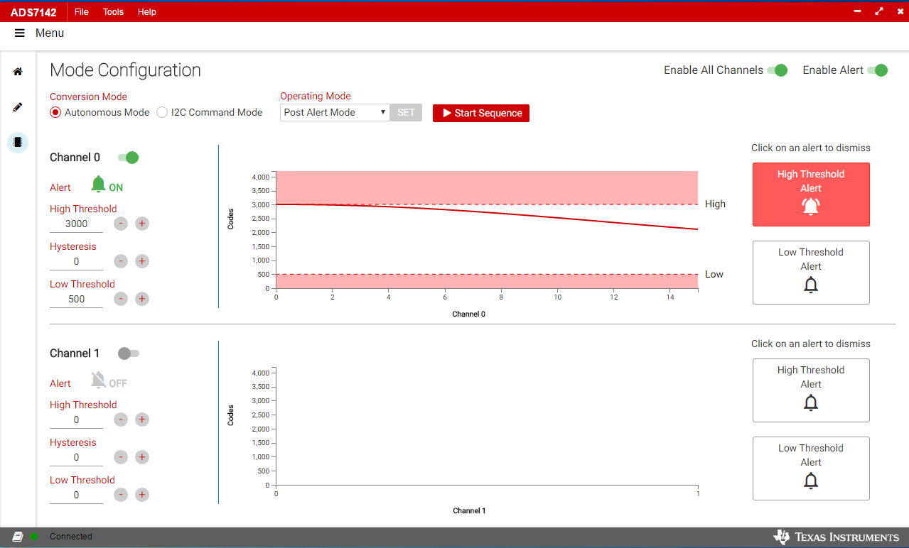 Figure 118. Post Alert Data Capture
8.2.2 Event-triggered PIR sensing with ADS7142
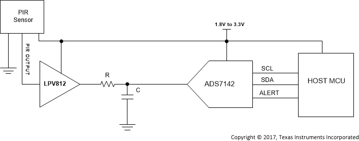 Figure 119. PIR Sensor with ADS7142
8.2.2.1 Design Requirements
A passive infrared (PIR) sensor is a commonly used sensor to detect motion by measuring infrared light emitted from any object that generates heat. PIR sensors are small, inexpensive, low-power, rugged, have a wide lens range, and are easy to use. PIR sensors are commonly used in security lighting and alarm systems used in indoor environments. When there is no motion or heat-emitting object in the vicinity of the sensor, the PIR sensor output is a DC voltage which is typically specified in the PIR datasheet. When a source of heat, such as a person or animal, comes into the sensor field of view, then the PIR sensor output changes. The amplitude of this signal is proportional to the speed and distance of the object relative to the sensor and is in the range of millivolts peak-to-peak. PIR sensors are often followed by a signal conditioning stage which amplifies the IR sensor output. A PIR sensor can be interfaced with the ADS7142 to make an ultra-low-power, autonomous PIR motion detector. The Autonomous Modes of the ADS7142 with threshold monitoring enables the system to put the host MCU into a low-power sleep mode and wake up the MCU only when motion is detected by the PIR sensor. Figure 119 shows a typical block diagram for an autonomous PIR motion detector using the ADS7142.
8.2.2.2 Detailed Design Procedure
The analog signal conditioning circuit is shown in the schematic in Figure 120. The first stage of the amplifier filter acts as a bandpass filter while the second stage applies an inverting gain. Components R10 and C5 serve as a low-pass filter to stabilize the supply voltage at the input to the sensor. Resistor R5 sets the bias current in the JFET output transistor of the PIR motion sensor. To save power, R5 is larger than recommended and essentially current starves the sensor. This comes at the expense of decreased sensitivity and higher output noise at the sensor output, which is a fair tradeoff for increased battery lifetime. Some of the loss in sensitivity at the sensor output can be compensated by a gain increase in the filter stages. Stage 1 of Figure 120 is arranged as a non-inverting gain filter stage. This provides a high-impedance load to the sensor so its bias point remains fixed. Because this stage has an effective DC gain of one due to C2, the sensor output bias voltage provides the DC bias for the first filter stage. Feedback diodes D1 and D2 provide clamping so that the op amps in both filter stages stay out of saturation for motion events which are close to the sensor. Stage 1 has a low and high cutoff frequency of 0.7 Hz and 10.6 Hz respectively and a gain of 220. Stage 2 is arranged as an inverting summer gain stage and is AC-coupled to Stage 1. A DC bias of VCC/2 is connected to the non-inverting input of the amplifier in this stage. Due to the higher gain in the filter stages and higher output noise from the sensor, care must be taken to optimize the placement of the high-frequency filter pole and the window comparator thresholds to avoid false detection.
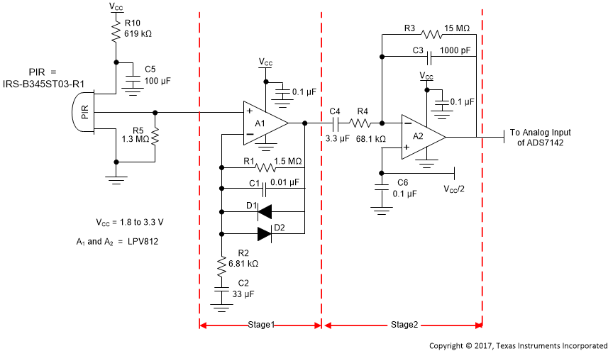 Figure 120. Signal Conditioning Circuit for PIR Sensor
8.2.2.3 Application Curves
When the PIR sensor detects motion, its output crosses the threshold and is detected by the ADS7142 as shown on Channel 1 in Figure 121.
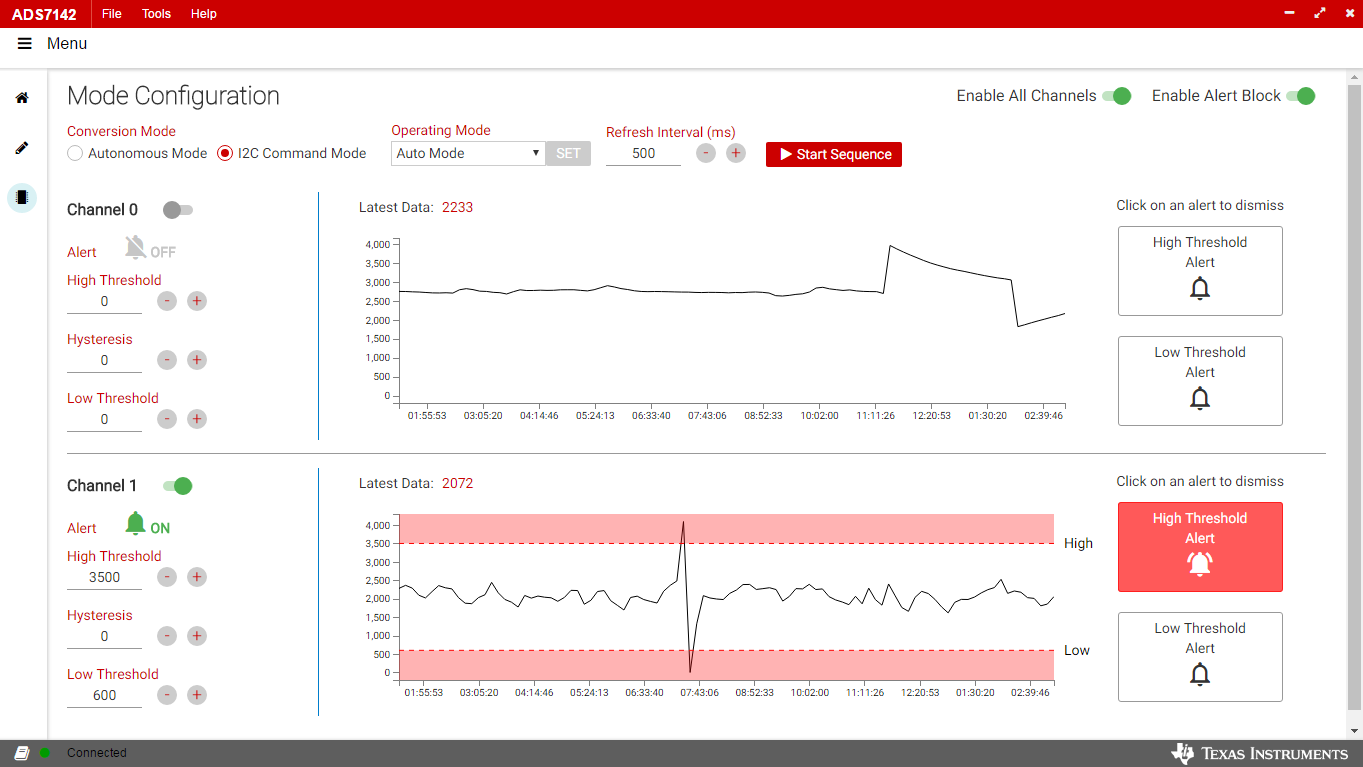 Figure 121. Alert Output from ADS7142 with PIR Sensor