SBAS773A September 2017 – December 2017 ADS7142
PRODUCTION DATA.
- 1 Features
- 2 Applications
- 3 Description
- 4 Revision History
- 5 Pin Configuration and Functions
-
6 Specifications
- 6.1 Absolute Maximum Ratings
- 6.2 ESD Ratings
- 6.3 Recommended Operating Conditions
- 6.4 Thermal Information
- 6.5 Electrical Characteristics - All Modes
- 6.6 Electrical Characteristics - Manual Mode
- 6.7 Electrical Characteristics - Autonomous Modes
- 6.8 Electrical Characteristics - High Precision Mode
- 6.9 Timing Requirements
- 6.10 Switching Characteristics
- 6.11 Typical Characteristics for All Modes
- 6.12 Typical Characteristics for Manual Mode
- 6.13 Typical Characteristics for Autonomous Modes
- 6.14 Typical Characteristics for High Precision Mode
-
7 Detailed Description
- 7.1 Overview
- 7.2 Functional Block Diagram
- 7.3 Feature Description
- 7.4 Device Functional Modes
- 7.5 Optimizing Power Consumed by the Device
- 7.6
Register Map
- 7.6.1 RESET REGISTERS
- 7.6.2 FUNCTIONAL MODE SELECT REGISTERS
- 7.6.3 INPUT CONFIG REGISTER
- 7.6.4 ANALOG MUX and SEQUENCER REGISTERS
- 7.6.5 OSCILLATOR and TIMING CONTROL REGISTERS
- 7.6.6 DATA BUFFER CONTROL REGISTER
- 7.6.7
ACCUMULATOR CONTROL REGISTERS
- 7.6.7.1 ACC_EN Register (address = 30h), [reset = 00h]
- 7.6.7.2 ACC_CH0_LSB Register (address = 08h), [reset = 00h]
- 7.6.7.3 ACC_CH0_MSB Register (address = 09h), [reset = 00h]
- 7.6.7.4 ACC_CH1_LSB Register (address = 0Ah), [reset = 00h]
- 7.6.7.5 ACC_CH1_MSB Register (address = 0Bh), [reset = 00h]
- 7.6.7.6 ACCUMULATOR_STATUS Register (address = 02h), [reset = 00h]
- 7.6.8
DIGITAL WINDOW COMPARATOR REGISTERS
- 7.6.8.1 ALERT_DWC_EN Register (address = 37h), [reset = 00h]
- 7.6.8.2 ALERT_CHEN (address = 34h), [reset = 00h]
- 7.6.8.3 DWC_HTH_CH0_MSB Register (address = 39h), [reset = 00h]
- 7.6.8.4 DWC_HTH_CH0_LSB Register (address = 38h), [reset = 00h]
- 7.6.8.5 DWC_LTH_CH0_MSB Register (address = 3Bh), [reset = 00h]
- 7.6.8.6 DWC_LTH_CH0_LSB Register (address = 3Ah), [reset = 00h]
- 7.6.8.7 DWC_HYS_CH0 (address = 40h), [reset = 00h]
- 7.6.8.8 DWC_HTH_CH1_MSB Register (address = 3Dh), [reset = 00h]
- 7.6.8.9 DWC_HTH_CH1_LSB Register (address = 3Ch), [reset = 00h]
- 7.6.8.10 DWC_LTH_CH1_MSB Register (address = 3Fh), [reset = 00h]
- 7.6.8.11 DWC_LTH_CH1_LSB Register (address = 3Eh), [reset = 00h]
- 7.6.8.12 DWC_HYS_CH1 (address = 41h), [reset = 00h]
- 7.6.8.13 PRE_ALT_MAX_EVENT_COUNT Register (address = 36h), [reset = 00h]
- 7.6.8.14 ALERT_TRIG_CHID Register (address = 03h), [reset = 00h]
- 7.6.8.15 ALERT_LOW_FLAGS Register (address = 0C), [reset = 00h]
- 7.6.8.16 ALERT_HIGH_FLAGS Register (address = 0Eh), [reset = 00h]
- 8 Application and Implementation
- 9 Power-Supply Recommendations
- 10Layout
- 11Device and Documentation Support
- 12Mechanical, Packaging, and Orderable Information
Package Options
Mechanical Data (Package|Pins)
- RUG|10
Thermal pad, mechanical data (Package|Pins)
Orderable Information
7 Detailed Description
7.1 Overview
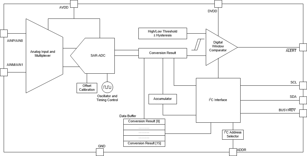
The ADS7142 is a nanopower, dual-channel, programmable sensor monitor with an integrated analog-to-digital converter (ADC), input multiplexer, digital comparator, data buffer, accumulator and internal oscillator. The input multiplexer can be either configured as two single-ended channels, one single-ended channel with remote ground sensing or one pseudo-differential channel where input can swing around AVDD/2. The device includes a Digital Window Comparator with a dedicated output pin, which can be used to alert the host when a programmed high or low threshold is crossed. The device address is configured by I2C Address Selector block. The device uses internal oscillators (High Speed or Low Power) for conversion. The start of conversion is controlled by the host in Manual Mode and by the device in Autonomous Modes.
The device also features a Data Buffer and an Accumulator. The data buffer can store up to 16 conversion results of the ADC in Autonomous Modes and the accumulator can accumulate up to 16 conversion results of ADC in High Precision Mode.
The device includes OFFSET Calibration for calibration of its own offset.
7.2 Functional Block Diagram
7.3 Feature Description
7.3.1 Analog Input and Multiplexer
Figure 39 shows a small-signal equivalent circuit for the analog input pins. The device includes a two-channel analog multiplexer with each input pin having ESD protection diodes to AVDD and GND. The sampling switches are represented by ideal switches SW1 and SW2 in series with resistors Rs1 and Rs2 (typically 150 Ω). The sampling capacitors, Cs1 and Cs2, are typically 15 pF. The multiplexer configuration is set by the CHANNEL_INPUT_CFG register.
During acquisition, switches SW1 and SW2 are closed to allow the input signal to charge the internal sampling capacitors.
During conversion, switches SW1 and SW2 are opened to disconnect the input signal from the sampling capacitors.
The analog input of the device are optimized to be driven by high impedance source (up-to 100 kΩ) in Autonomous Modes or in High Precision Mode mode with low power oscillator. It is recommended to drive the analog input of the device with an external amplifier when in Autonomous Modes or in High Precision Mode mode with High Speed oscillator. Figure 30 and Figure 31 provide the analog input current for CH0 and CH1 of the device.
Figure 40, Figure 41 and Figure 42 provide a simplified circuit for analog input for input configurations described in Two-Channel, Single-Ended Configuration, Single-Channel, Single-Ended Configuration and Single-Channel, Pseudo-Differential Configuration respectively. The analog multiplexer supports following input configurations (set by writing into CHANNEL_INPUT_CFG register).
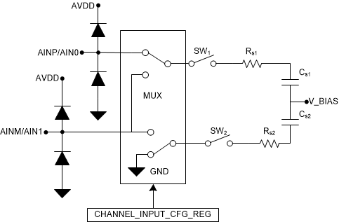 Figure 39. Equivalent Circuit for Analog Input
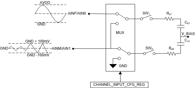 Figure 41. Single-Channel, Single-Ended Configuration with Remote Ground Sensing
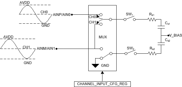 Figure 40. Two-Channel, Single-Ended Configuration
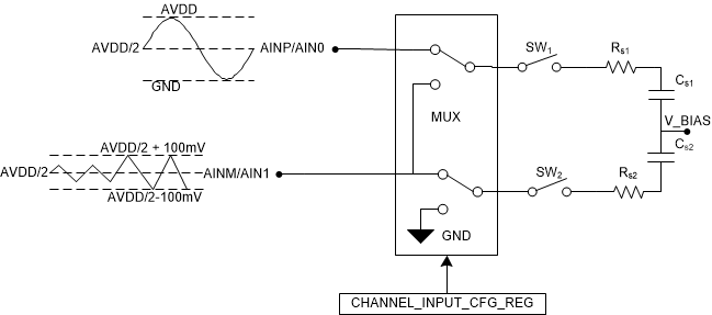 Figure 42. Single-Channel, Pseudo-Differential Configuration
7.3.1.1 Two-Channel, Single-Ended Configuration
Refer to Figure 40 for a simplified block diagram showing a two-channel, single ended configuration. Set CH0_CH1_IP_CFG bits = 00b or 11b to select this configuration. This is also the default configuration of the device after power up. In this configuration, CS2 always samples the GND pin and CS1 samples the input signal provided on Channel 0 (AINP/AIN0) or Channel 1 (AINM/AIN1) based on the channel selection. Each analog input channel can accept input signals in the range 0 V to AVDD V.
On power-up, the device wakes up in manual mode with Two-Channel, Single-Ended Configuration and samples CH0 only. This configuration can also be set by setting OPMODE_SEL to 000b or 001b,
The device can be configured to sample either CH0 or CH1 or both channels by setting bits in AUTO_SEQ_CHEN register to select the channels.
- To select a channel in AUTO sequence, set AUTO_SEQ_CHx bit in AUTO_SEQ_CHEN register to 1.
- Set bits in OPMODE_SEL register to 100b or 101b for Manual Mode with AUTO sequence.
- Set bits in OPMODE_SEL register to 110b for Autonomous Modes with AUTO sequence.
- Set bits in OPMODE_SEL register to 111b for High Precision Mode with AUTO sequence.
7.3.1.2 Single-Channel, Single-Ended Configuration
Refer to Figure 41 for a simplified block diagram showing a single-channel, single ended configuration. Set CH0_CH1_IP_CFG bits = 01b to select this configuration. In this configuration, CS1 samples the input signal provided on the AINP/AIN0 pin whereas CS2 samples input signal provided on the AINM/AIN1 pin. AINP/AIN0 pin can accept input signals in the range 0 V to AVDD V and AINM/AIN1 pin can accept input signals in the range –100 mV to +100 mV. This input configuration is useful in systems where the sensor and/or the signal conditioning block is placed far from the device and there could be a small difference between the ground potentials. In this channel configuration, remove channel 1 from AUTO sequence by setting the AUTO_SEQ_CH1 bit to 0. Selecting channel 1 in AUTO sequence leads to an error condition and the device sets an error flag in SEQUENCE_STATUS register.
7.3.1.3 Single-Channel, Pseudo-Differential Configuration
Refer to Figure 42 for a simplified block diagram showing a single-channel, pseudo-differential configuration. Set CH0_CH1_IP_CFG bits = 10b to select this configuration. In this configuration, CS1 samples the input signal provided on the AINP/AIN0 pin whereas CS2 samples input signal provided on the AINM/AIN1 pin. AINP/AIN0 pin can accept input signals in the range 0 V to AVDD V and AINM/AIN1 pin can accept input signals in the range (AVDD/2) - 100 mV to (AVDD/2) + 100 mV. This input configuration is useful to interface with sensors that provide pseudo-differential signal with negative output as AVDD/2 like an electrochemical gas sensor. In this channel configuration, remove channel 1 from AUTO sequence by setting the AUTO_SEQ_CH1 bit to 0. Selecting channel 1 in AUTO sequence leads to an error condition and the device sets an error flag in SEQUENCE_STATUS register.
7.3.2 OFFSET Calibration
The offset can be calibrated by setting the TRIG_OFFCAL bit in OFFSET_CAL register. During offset calibration, the sampling switches are open (Figure 39) and the device keeps BUSY/RDY pin high. The device calculates its offset error and corrects for this error for subsequent conversions. The device calibrates the offset on power up. To nullify the change in offset due to change in temperature or in AVDD voltage, it is recommended to perform this calibration periodically.
7.3.3 Reference
The device uses the analog supply voltage (AVDD) as a reference for the analog-to-digital conversion process. It is recommended to place a 220-nF, low-ESR ceramic decoupling capacitor between the AVDD pin and the GND pin, close to the AVDD Pin. Refer to Power-Supply Recommendations section.
7.3.4 ADC Transfer Function
The ADC provides data in straight binary format. The ADC resolution can be computed by Equation 1:
where
- VREF = AVDD
- N = 12 for Autonomous Monitoring Modes and Manual Mode
Figure 43 and Figure 44 show the ideal transfer characteristics for Single-Ended Input and Pseudo-Differential Input, respectively. Table 1 show the digital output codes for the transfer functions.
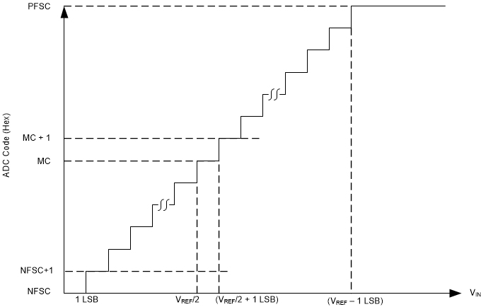 Figure 43. Ideal Transfer Characteristics for Single-Ended Configurations
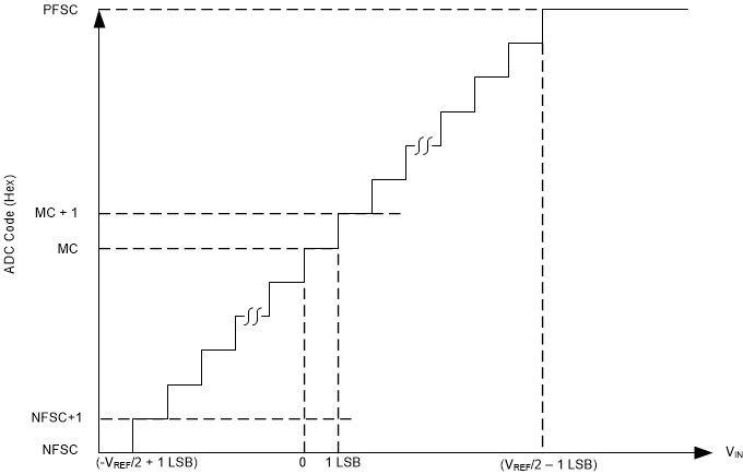 Figure 44. Ideal Transfer Characteristics for Pseudo-Differential Configuration
Table 1. Transfer Characteristics
| INPUT VOLTAGE for SINGLE ENDED INPUT | INPUT VOLTAGE for PSEUDO DIFFERENTIAL INPUT | CODE | DESCRIPTION | IDEAL OUTPUT CODE |
|---|---|---|---|---|
| Autonomous Monitoring Mode Or Manual Mode | ||||
| ≤1 LSB | ≤(-VREF/2 + 1) LSB | NFSC | Negative full-scale code | 000 |
| 1 LSB to 2 LSBs | (-VREF/2 + 1) to (-VREF/2 + 2) LSB | NFSC + 1 | — | 001 |
| (VREF / 2) to (VREF / 2) + 1 LSB | 0 to 1 LSB | MC | Mid code | 800 |
| (VREF / 2) + 1 LSB to (VREF / 2) + 2 LSBs | 1 to 2 LSB | MC + 1 | — | 801 |
| ≥ VREF – 1 LSB | ≥ VREF/2 – 1 LSB | PFSC | Positive full-scale code | FFF |
7.3.5 Oscillator and Timing Control
The device uses one of the two internal oscillators (Low Power Oscillator or High Speed Oscillator) for converting the analog input voltage into a digital output code.
The steps for selecting the oscillator and setting the sampling speed are listed below:
- Select the Low Power Oscillator (OSC_SEL = 1b) to monitor slow moving signals(< 300 Hz) at extremely low power consumption and sampling speeds (< 600 SPS). Select the High Speed Oscillator (OSC_SEL = 0b) to scan the sensor signals with faster sampling speed (> 50 kHz).
- Set sampling speed by programming the nCLK register:

where
- fs = Sampling Speed
- Oscillator Frequency = 1/tHSO or 1/tLPO depending on the OSC_SEL bit, refer the Specifications for 1/tHSO or 1/tLPO.
- nCLK is number of clocks in one conversion cycle (nCLK register)
7.3.6 I2C Address Selector
The I2C address for the device is determined by connecting external resistors on ADDR pin. The device address are selected on power-up based on the resistor values. The device retains this address until the next power up, or until next device reset, or until the device receives a command to program its own address (General Call with Write Software programmable part of slave address). Figure 45 provides the connection diagram for the ADDR pin and Table 2 provides the resistor values for selecting different addresses of the device.
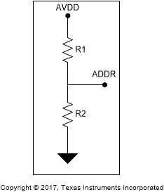 Figure 45. External Resistor Connection Diagram for ADDR Pin
Table 2. I2C Address Selection
| Resistors | Address | |
|---|---|---|
| R1 (2) | R2(2) | |
| 0 Ω | DNP(1) | 0011111b (1Fh) |
| 11 kΩ | DNP(1) | 0011110b (1Eh) |
| 33 kΩ | DNP(1) | 0011101b (1Dh) |
| 100 kΩ | DNP(1) | 0011100b (1Ch) |
| DNP(1) | 0Ω or DNP(1) | 0011000b (18h) |
| DNP(1) | 11 kΩ | 0011001b (19h) |
| DNP(1) | 33 kΩ | 0011010b (1Ah) |
| DNP(1) | 100 kΩ | 0011011b (1Bh) |
7.3.7 Data Buffer
When operating in Autonomous Monitoring Mode, the device can use the internal data buffer for data storage. The internal data buffer is 16-bit wide and 16-word deep and follows the FIFO (first-in, first-out) approach.
7.3.7.1 Filling of the Data Buffer
The write operation to the data buffer starts and stops as per the settings in the DATA_BUFFER_OPMODE register. The DATA_BUFFER_STATUS register provides the number of entries filled in the data buffer and this register can be read during an active sequence to get the current status of the data buffer.
The time between two consecutive conversions is set by the nCLK register and Equation 3 provides the relationship for time between two consecutive conversions of the same channel and nCLK parameter.
where
- tcc is time between two consecutive conversions of same channel, tcc = k × tcycle .
- k is number of channels enabled in the device sequence.
- nCLK is number of clocks used by device for one conversion cycle.
- Oscillator Timer Period is tLPO or tHSO depending on OSC_SEL value . Refer to the Specifications for tLPO or tHSO .
The format of the 16-bit contents of each entry in the data buffer are set by programming the DATA_OUT_CFG register. The DATA_OUT_CFG register enables the Channel ID and DATA_VALID flag in data buffer. Channel ID represents the channel number for the data entry in the data buffer. DATA_VALID is set to zero in either of the following conditions:
- If the entry in the data buffer is not filled after the last start of sequence.
- If the I2C master tries to read more than 16 entries from the data buffer, device provides zeros with DATA_VALID set to zero.
At the end of the write operation, the data buffer always has results of 16 (or lesser) consecutive conversions. The data buffer is filled in the order that the data is converted by the ADC. The channels converted by the ADC are controlled by the AUTO_SEQ_CHEN register. The entries that are not filled during an active sequence are filled with zeros.
7.3.7.2 Reading data from the Data Buffer
The device brings the BUSY/RDY pin low after completion of the sequence or after the SEQ_ABORT bit is set. As illustrated in Figure 46, the device provides the contents of the data buffer (in FIFO fashion) on receiving I2C read frame, which consists of the device address and the read bit set to 1.
 Figure 46. Reading Data Buffer (16 Bit Words × 16 Words)
The device returns zeroes with DATA VALID flag set to zero for all I2C read frames received after all the valid data words from the data buffer are read or when a I2C read frame is issued during an active sequence (indicated by high on the BUSY/RDY pin). The I2C master needs to provide a NACK followed by a STOP or RESTART condition in an I2C frame to finish the reading process. The data buffer is reset by setting the SEQ_START bit or after resetting the device.
7.3.8 Accumulator
When operating in High Precision Mode, the device offers a 16-bit internal accumulator per channel. The Accumulator for a channel is enabled only if that channel is selected in the channel scanning sequence. The accumulator adds sixteen 12-bit conversion results. The result of adding 16 twelve bit words is one 16 bit word that has an effective resolution of an 16-bit ADC. The time between two consecutive conversions for accumulation is controlled by the nCLK register and Equation 3 provides the relationship for time between two consecutive conversions of same channel and nCLK parameter.
The accumulated data can be read from the ACCUMULATOR_DATA registers in the device.
ACCUMULATOR_STATUS register provides the number of accumulations done in the accumulator since last conversion. This register can be read during an active sequence to get the current status of the accumulator.
The accumulator is reset on setting the SEQ_START bit and on resetting the device.
Equation 4 provides the relationship between high precision data and ADC conversion results.

Equation 5 provides the value of LSB in high precision mode for the accumulated result.

7.3.9 Digital Window Comparator
The internal Digital Window Comparator is available in all modes. In Autonomous Modes with Thresholds monitoring and Diagnostics, the digital window comparator controls the filling of the data and the output of the alert pin and in other modes, it only controls the output of the alert pin. Figure 47 provides the block diagram for digital window comparator.
 Figure 47. Digital Comparator Block Diagram
The Low Side Threshold, High Side Threshold, and Hysteresis parameters are independently programmable for each input channel. Figure 48 shows the comparison thresholds and hysteresis for the two comparators. A Pre-Alert event counter after each comparator counts the output of the comparator and sets the latched flags. The Pre-Alert Event Counter settings are common to the two channels.
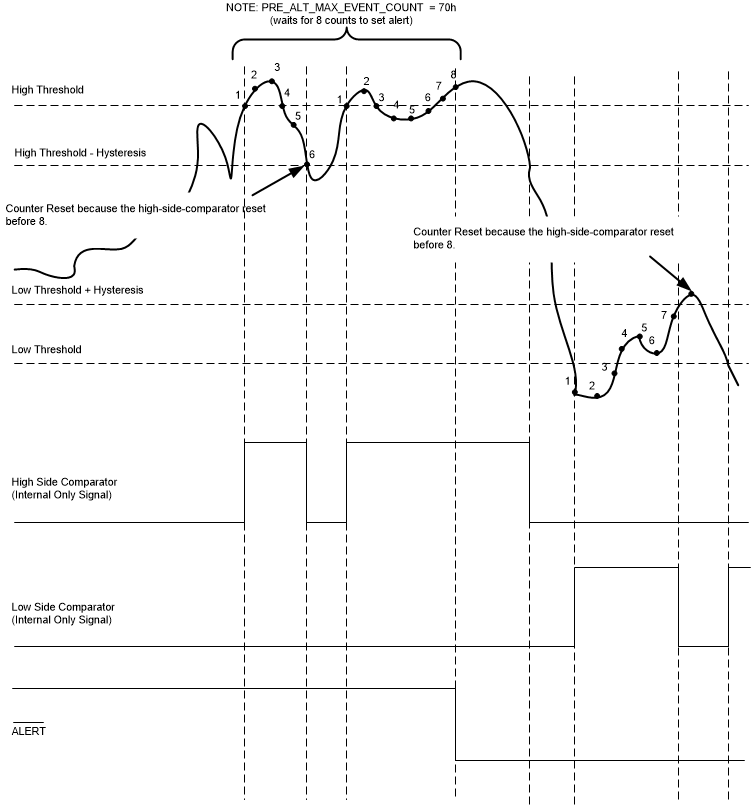 Figure 48. Thresholds, Hysteresis and Event Counter for Digital Window Comparator
DWC_BLOCK_EN bit in ALERT_DWC_EN register enables/disables the complete Digital Window Comparator block (disabled at power-up) and ALERT_EN_CHx bits in ALERT_CHEN register enables Digital Window Comparator for individual channels. Once enabled, whenever a new conversion result is available:
- The output of the high side comparator transitions to logic high when the conversion result is greater than the High Threshold. This comparator resets when the conversion result is less than the High Threshold – Hysteresis.
- The output of the low side comparator transitions to logic high when the conversion result is less than the Low Threshold. This comparator resets when the conversion result is greater than the Low Threshold + Hysteresis.
- A different threshold and hysteresis can be used for each channel.
- Once the output of either the high side or low side comparator transitions high the Pre-Alert Event Counter begins to increment for each subsequent conversion. This counter continues to increment until it reaches the value stored in the PRE_ALT_MAX_EVENT_COUNT register. Once it reaches PRE_ALT_MAX_EVENT_COUNT, the Alert becomes active and sets the latched flags. If the comparator output becomes zero before counter reaches PRE_ALT_MAX_EVENT_COUNT, then the event counter is reset to zero, Alert does not be set and lateched flag is not set.
Therefore, the latched flags (high and low) for the channel are updated only if the respective comparator output remains 1 for the specified number of consecutive conversions (set by the PRE_ALT_MAX_EVENT_COUNT).
The latched flags can be read from the ALERT_LOW_FLAGS and ALERT_HIGH_FLAGS registers. To clear a latched flag, write 1 to the applicable bit location. The ALERT pin status is re-evaluated whenever an applicable latched flag gets set or is cleared.
The response time for ALERT pin can be estimated by Equation 6
where
- k is number of channels enabled in device sequence
- nCLK is number of clocks used by device for one conversion cycle.
- Oscillator Timer Period is tLPO or tHSO depending on OSC_SEL value . Refer to the Specifications for tLPO or tHSO .
7.3.10 I2C Protocol Features
7.3.10.1 General Call
On receiving a general call (00h), the device provides an ACK.
7.3.10.2 General Call with Software Reset
On receiving a general call (00h) followed with Software Reset (06h), the device resets itself.
7.3.10.3 General Call with Write Software programmable part of slave address
On receiving a general call (00h) followed by 04h, the device configures its own I2C address configured by the ADDR pin. During this operation, the device keeps BUSY/RDY Pin high and does not respond to other I2C commands except general call.
7.3.10.4 Configuring Device into High Speed I2C mode
The device can be configured in High Speed I2C mode by providing an I2C frame with one of the HS-mode master codes (08h to 0Fh).
After receiving one of the HS-mode master codes, the device sets the HS_MODE bit in OPMODE_I2CMODE_STATUS register and remains in High Speed I2C mode until a STOP condition is received in an I2C frame.
7.3.10.5 Bus Clear
If the SDA line is stuck LOW due to an incomplete I2C frame, providing nine clocks on SCL is recommended. The device releases the SDA line within these nine clocks, and then the next I2C frame can be started.
7.3.11 Device Programming
Table 3 provides the acronyms for different conditions in an I2C Frame.
Table 3. I2C Frame Acronyms
| Symbol | Description |
|---|---|
| S | Start condition for I2C Frame |
| Sr | Re-start condition for I2C Frame |
| P | Stop condition for I2C Frame |
| A | ACK (Low) |
| N | NACK (High) |
| R | Read Bit (High) |
| W | Write Bit (Low) |
Table 4. Opcodes for Commands
| Opcode | Command Description |
|---|---|
| 00010000b | Single Register Read |
| 00001000b | Single Register Write |
| 00011000b | Set Bit |
| 00100000b | Clear Bit |
| 00110000b | Reading a continuous block of registers |
| 00101000b | Writing a continuous block of registers |
7.3.11.1 Reading Registers
The I2C master can either read a single register or a continuous block registers from the device as described in Single Register Read and in Reading a Continuous Block of Registers.
7.3.11.1.1 Single Register Read
To read a single register from the device, the I2C master has to first provide an I2C command with three frames (of 8-bits each) to set the address as illustrated in Figure 49. The register address is the address of the register which must be read. The opcode for register read command is listed in Table 4.
 Figure 49. Setting Register Address for Reading Registers
After this, the I2C master has to provide another I2C frame containing the device address and read bit as illustrated in Figure 50. After this frame, the device provides register data. If the host provides more clocks, the device provides same register data. To end the register read command, the master has to provide a STOP or a RESTART condition in the I2C frame.
 Figure 50. Reading Register Data
7.3.11.1.2 Reading a Continuous Block of Registers
To read a continuous block of registers, the I2C master has to first provide an I2C command to set the address as illustrated in Figure 49. The register address is the address of the first register in the block which must be read. The opcode for reading a continuous block of register is listed in Table 4.
Next, the I2C master has to provide another I2C frame containing the device address and read bit as illustrated in Figure 51. After this frame, the device provides register data. On providing more clocks, the device provides data for next register. On reading data from addresses which does not exist in the Register Map of the device, the device returns zeros. If the device does not have any further registers to provide the data, it provides zeros. To end the register read command, the master has to provide a STOP or a RESTART condition in the I2C frame.
 Figure 51. Reading a Continuous Block of Registers
7.3.11.2 Writing Registers
The I2C master can either write a single register or a continuous block registers to the device. It can also set a few bits in a register or clear a few bits in a register.
7.3.11.2.1 Single Register Write
To write to a single register in the device, the I2C master has to provide an I2C command with four frames as illustrated in Figure 52. The register address is the address of the register which must be written and register data is the value that must be written. The opcode for single register write is listed in Table 4. To end the register write command, the master has to provide a STOP or a RESTART condition in the I2C frame.
 Figure 52. Writing a Single Register
7.3.11.2.2 Set Bit
To set bits in a register without changing the other bits, the I2C master has to provide an I2C command with four frames as illustrated in Figure 52. The register address is the address of the register in which the bits needs to be set and register data is the value representing the bits which need to be set. Bits with value as 1 in register data are set and bits with value as 0 in register data are not changed. The opcode for set bit is listed in Table 4. To end this command, the master has to provide a STOP or RESTART condition in the I2C frame.
7.3.11.2.3 Clear Bit
To clear bits in a register without changing the other bits, the I2C master has to provide an I2C command with four frames as illustrated in Figure 52. The register address is the address of the register in which the bits needs to be cleared and register data is the value representing the bits which need to be cleared. Bits with value as 1 in register data are cleared and bits with value as 0 in register data are not changed. The opcode for clear bit is listed in Table 4. To end this command, the master has to provide a STOP or a RESTART condition in the I2C frame.
7.3.11.2.4 Writing a continuous block of registers
To write to a continuous block of registers, the I2C master has to provide an I2C command as illustrated in Figure 53. The register address is the address of the first register in the block which needs to be written. The I2C master has to provide data for registers in subsequent I2C frames in an ascending order of register addresses. Writing data to addresses which do not exist in the Register Map of the device has no effect. The opcode for writing a continuous block of registers is listed in Table 4. If the data provided by the I2C master exceeds the address space of the device, the device neglects the data beyond the address space. To end the register write command, the master has to provide a STOP or a RESTART condition in the I2C frame.
 Figure 53. Writing a continuous block of registers
7.4 Device Functional Modes
The device has below functional modes:
- Manual Mode
- Autonomous Modes
- Autonomous Mode with Threshold Monitoring and Diagnostics.
- Autonomous Mode with Burst Data
- High Precision Mode
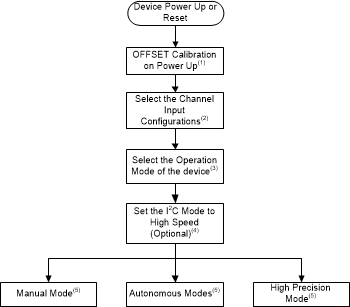
Device powers up in Manual Mode and can be configured into one of the other modes of these modes by writing the configuration registers for the desired mode. Steps for configuring device into different modes are illustrated in Figure 54
7.4.1 Device Power Up and Reset
On power up, the device calibrates its own offset and calculates the address from the resistors connected on ADDR pin. During this time, the device keeps BUSY/RDY high.
The device can be reset by recycling power on AVDD pin, by General Call(00h) followed by software reset (06h), or by writing the WKEY register followed by setting the bit in DEVICE_RESET register.
Recycling power on the AVDD pin and on General call(00h) followed by software reset (06h), all the device configurations are reset, and the device initiates offset calibration and re-evaluates its I2C address.
When setting the bit in DEVICE_RESET register, all the device configurations except latched flags for the Digital Window Comparator and WKEY register are reset, The device does not initiate offset calibration and does not re-evaluate its I2C address.
7.4.2 Manual Mode
On power-up, the device is in Manual Mode using the single ended and dual channel configuration and starts by sampling the analog input applied on Channel 0. In this mode, the device uses the high frequency oscillator for conversions. Manual mode allows the external host processor to directly request and control when the data is sampled. The data capture is initiated by an I2C command from the host processor and the data is then returned over the I2C bus at a throughput rate of up to 140-kSPS. Applications that could take advantage of this type of functionality include traditional ADC applications that require 1 or 2 channels of continuous data output.
After setting the operation mode to Manual Mode as illustrated in Figure 54, steps for operating the device to be in Manual Mode and reading data are illustrated in Figure 55. The host can either configure the device to scan through one channel or both channels by configuring the CHANNEL_INPUT_CFG register and AUTO_SEQ_CFG register.
7.4.2.1 Manual Mode with CH0 Only
Set the OPMODE_SEL register to 000b or 001b for Manual Mode with CH0 only. The host has to provide device address and read bit to start the conversions. To continue with conversions and reading data to the host must provide continuous SCL (Figure 56). In this mode, a NACK followed by a STOP condition in I2C frame is required to abort the operation. Then the device operation mode can be changed to another operation mode.
7.4.2.2 Manual Mode with AUTO Sequence
Set the OPMODE_SEL register to 100b or 101b for Manual Mode with AUTO Sequence. The host has to set the SEQ_START bit in START_SEQUENCE register and provide the device address and read bit to start the conversions. To continue with conversions and reading data, the host must provide continuous SCL (Figure 56). In this mode, the SEQ_ABORT bit in ABORT_SEQUENCE register must be set to abort the operation. Then the device operation mode can be changed to another operation mode. In this mode, a register read aborts the AUTO sequence.
In Manual Mode, the device always uses the High Speed Oscillator and the nCLK parameter has no effect. The maximum scan rate is given by Equation 7:

where
- fs = Maximum sampling Speed in kSPS
- TSCL= Time period of SCL clock (in µsec)
- if TSCL-LOW (Low period of SCL) < 1.8.µsec, k = (1.8 - TSCL-LOW) and Device stretches clock in Manual Mode. Not Applicable for Standard I2C Mode (100 kHz).
- if TSCL-LOW (Low period of SCL) ≥ 1.8.µsec, k = 0 and Device does not stretch clock in Manual Mode.
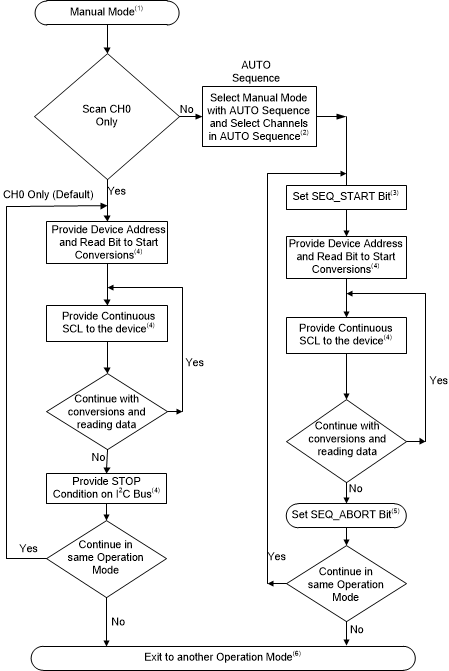
Data can be read from the device by providing a device address and read bit followed by continuous SCL as shown in Figure 56.

7.4.3 Autonomous Modes
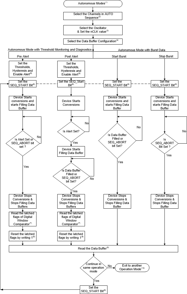
In Autonomous Mode, the device can be programmed to monitor the voltage applied on the analog input pins of the device and generate a signal on the ALERT pin when the programmable high or low threshold values are crossed and store the conversion results in the data buffer before or after the crossing a threshold or before setting the SEQ_ABORT bit (Start Burst) or after setting the START_SEQUENCE bit.
In Autonomous mode, the device generates the start of conversion using the internal oscillator. The first start of conversion must be provided by the host and the device generates the subsequent start of conversions.
After configuring the operation mode to autonomous mode (Set OPMODE_SEL register to 110b) as illustrated in Figure 54, steps for operating the device to be in different autonomous modes are illustrated in Figure 57
TI recommends aborting the present sequence by setting the SEQ_ABORT bit before changing the device operation mode or device configuration.
7.4.3.1 Autonomous Mode with Threshold Monitoring and Diagnostics
The Threshold Monitoring Mode automatically scans the input voltage on the input channel(s) and generates a signal when the programmable high or low threshold values are crossed. This mode is useful for applications where the output of the sensor needs to be continuously monitored and action only taken when the sensor output deviates outside of an acceptable range. Applications that could take advantage of this type of functionality include wireless sensor nodes, environmental sensors, smoke and heat detectors, motion detectors, and so on.
In this mode, the data buffer can be configured to store the conversion results of the ADC in two different ways.
7.4.3.1.1 Autonomous Mode with Pre Alert Data
In this mode, the device stores the sixteen conversion prior to the activation of the Alert. Upon activation of Alert, conversion stops. For this mode, Set DATA_BUFFER_OPMODE to 100b. In this mode, the device starts converting and stores the data on setting the bit in the SEQ_START register and continues to store the data into the data buffer until one of the digital comparator flags is set for crossing a high threshold or a low threshold for the channels selected in the sequence. If the SEQ_ABORT bit is set before the data buffer is filled, the device aborts the sequence and stops storing the conversion results. If more than 16 conversions occur between start of sequence and alert output, the first entries written into the data buffer are over-written.
Figure 58 and Figure 59 illustrates the filling of data buffer in autonomous mode with Pre alert Data.
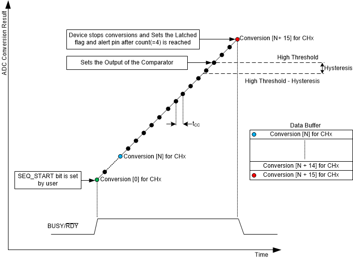 Figure 58. Pre Alert Data for Single Channel Configurations
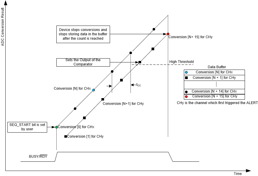 Figure 59. Pre Alert Data for Dual Channel Configuration
7.4.3.1.2 Autonomous Mode with Post Alert Data
In this mode, the device captures the next sixteen conversion results after the Alert is active. Once these sixteen conversions are stored in the data buffer, all conversion stops. For this mode, Set DATA_BUFFER_OPMODE to 110b. In this mode, the device starts converting the data on setting the SEQ_START bit and stores the data in the data buffer when one of the digital comparator flags is set after the crossing a high threshold or a low threshold for the channels selected in the sequence. if the SEQ_ABORT bit is set before the data buffer is filled, the device aborts the sequence and stops storing the conversion results.
Figure 60 and Figure 61 illustrates the filling of the data buffer in autonomous mode with Post Alert Data.
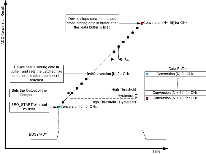 Figure 60. Post Alert Data for Single Channel Configurations
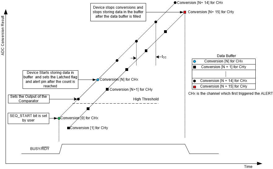 Figure 61. Post Alert Data for Dual Channel Configuration
7.4.3.2 Autonomous Mode with Burst Data
In this mode, the device can be configured to store up-to 16 conversion results in the data buffer based on user command. Applications that could take advantage of this mode are remote data loggers, environmental sensing and patient monitors. In this mode, the user can either start the burst or stop the burst of data as described in the following sections:
7.4.3.2.1 Autonomous Mode with Start Burst
For this mode, set DATA_BUFFER_OPMODE to 001b. With Start Burst, the user can configure the device to start the filling of data buffer with conversion results by setting the SEQ_START bit and the device stops converting data and filling the data buffer after the data buffer is filled.
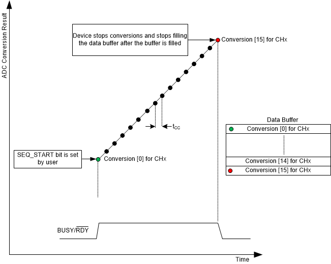 Figure 62. Start Burst with Single Channel Configurations
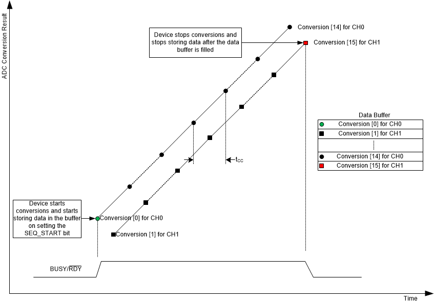 Figure 63. Start Burst with Dual Channel Configuration
7.4.3.2.2 Autonomous Mode with Stop Burst
For this mode, Set DATA_BUFFER_OPMODE to 000b. With Stop Burst, the user can configure the device to stop filling the data buffer with conversion results by setting the SEQ_ABORT bit. If more than 16 conversions occur between start of sequence and abort of sequence, the entries first written into the data buffer are over-written. Figure 64 and Figure 65 illustrate the filling of the data buffer in autonomous mode with Stop Burst.
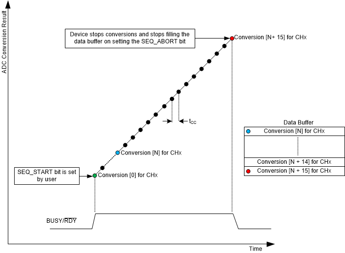 Figure 64. Stop Burst with Single Channel Configurations
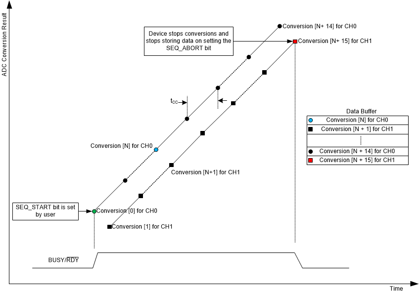 Figure 65. Stop Burst with Dual Channel Configuration
7.4.4 High Precision Mode
The High Precision Mode increases the accuracy of the data measurement to 16-bit accuracy. This is useful for applications where the level of precision required to accurately measure the sensor output needs to be higher than 12 bits. Applications that could take advantage of this type of functionality include gas detectors, air quality testers, water quality testers, and so on.
For this mode, Set OPMODE_SEL register to 111b. In this mode, the device starts converting and starts accumulating the conversion results in an accumulator on setting the SEQ_START bit. The device stops accumulating the conversion results in accumulator after 16 conversions or when the SEQ_ABORT bit is set. Upon accumulating 16 twelve bit conversions, the accumulator contains one 16 bit conversion result. The device has an accumulator for each channel and the device accumulates conversion results from each channel into the respective accumulator. If the operation of the device is aborted in high precision mode before the BUSY/RDY pin goes low, the device provides invalid data. In this mode, on providing a device address and read bit for reading data buffer (Figure 46), the device provides zeroes as output. In this mode, the BUSY/RDY can be used to wake up the MCU or host from sleep or hibernation on completion of accumulation. The steps for configuring the device into High Precision Mode are illustrated in Figure 66 .
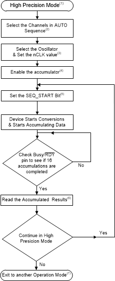
It is recommended to abort the present sequence by setting the SEQ_ABORT bit before changing the device operation mode or device configuration.
Figure 67 illustrates the accumulation of conversion results in high precision mode.
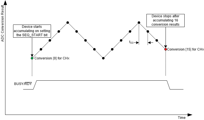 Figure 67. High Precision Mode with Single Channel Configurations
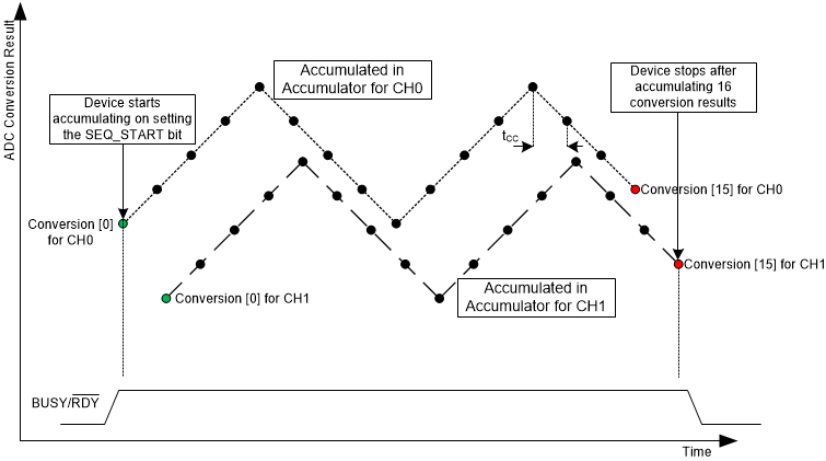 Figure 68. High Precision Mode with Dual Channel Configurations
7.5 Optimizing Power Consumed by the Device
- Keep the analog supply voltage (AVDD) as close as possible to the analog input signal to the device. Set AVDD to be greater than or equal to the analog input signal to the device.
- Keep the digital supply voltage (DVDD) at the lowest permissible value.
- In Manual Mode, run the device at the optimum sampling speed. Power consumption scales with Sampling Speed. In Manual Mode, the sampling speed is dependent on time period (or frequency) of SCL (Equation 7). Figure 69 and Figure 70 illustrate scaling of IAVDD and IDVDD with SCL in Manual Mode.
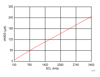
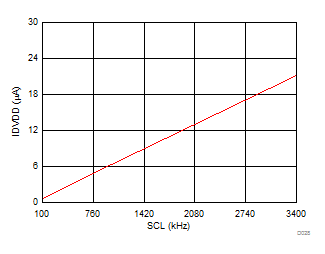
| DVDD = 3.3 V |
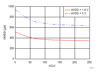
- In Autonomous Modes and High Precision Mode, the balance between sampling speed and power consumption can be obtained by selecting the oscillator for conversion and setting the nCLK value. The device sampling speed and power consumption reduce by increasing the nCLK value. Refer to Figure 71, Figure 72, Figure 73 and Figure 74 for current consumption in Autonomous modes and High Precision mode with different nCLK values.
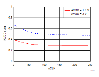
| Stop Burst Mode | With Low Power Oscillator | |
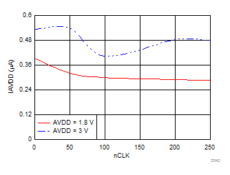
| With Low Power Oscillator | ||
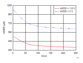
| Stop Burst Mode | With High Speed Oscillator | |
| With High Speed Oscillator | ||
7.6 Register Map
Table 5 provides the list of registers in the device. All the registers reset to their default values on power up and on receiving a General Call with Software Reset. (See Reset section).
Table 5. Register Map
| S.NO. | ADDRESS | REGISTER NAME | REGISTER DESCRIPTION |
|---|---|---|---|
| RESET REGISTERS | |||
| 1 | 17h | WKEY | Write Key for writing into DEVICE_RESET register |
| 2 | 14h | DEVICE_RESET | Resets the device |
| FUNCTIONAL MODE SELECT REGISTERS | |||
| 3 | 15h | OFFSET_CAL | Initiates Internal Offset Calibration Cycle |
| 4 | 1Ch | OPMODE_SEL | Sets the operation mode and enables auto-sequencing |
| 5 | 00h | OPMODE_I2CMODE_STATUS | Provides the present Operating Mode and I2C mode information |
| INPUT CONFIG REGISTER | |||
| 6 | 24h | CHANNEL_INPUT_CFG | Configures the analog input channels |
| ANALOG MUX and SEQUENCER REGISTERS | |||
| 7 | 20h | AUTO_SEQ_CHEN | Enables Auto sequencing for selected channels |
| 8 | 1Eh | START_SEQUENCE | Starts the channel scanning sequence |
| 9 | 1Fh | ABORT_SEQUENCE | Aborts the channel scanning sequence |
| 10 | 04h | SEQUENCE_STATUS | Provides the status of sequence in device |
| OSCILLATOR and TIMING CONTROL REGISTERS | |||
| 11 | 18h | OSC_SEL | Selects the oscillator for the conversion process |
| 12 | 19h | nCLK_SEL | Sets the nCLK for the device |
| DATA BUFFER CONTROL REGISTER | |||
| 13 | 2Ch | DATA_BUFFER_OPMODE | Selects Data Buffer operation mode |
| 14 | 28h | DOUT_FORMAT_CFG | Configures the data output format for data buffer |
| 15 | 01h | DATA_BUFFER_STATUS | Provides the present status of Data Buffer |
| ACCUMULATOR CONTROL REGISTERS | |||
| 16 | 30h | ACC_EN | Enables the Accumulator |
| 17 | 08h | ACC_CH0_LSB | Provides the LSB of accumulated data for CH0 (Read Only) |
| 18 | 09h | ACC_CH0_MSB | Provides the MSB of accumulated data for CH0 (Read Only) |
| 19 | 0Ah | ACC_CH1_LSB | Provides the LSB of accumulated data for CH1 (Read Only) |
| 20 | 0Bh | ACC_CH1_MSB | Provides the MSB of accumulated data for CH1 (Read Only) |
| 21 | 02h | ACCUMULATOR_STATUS | Provides the present status of Accumulator |
| DIGITAL WINDOW COMPARATOR REGISTERS | |||
| 22 | 37h | ALERT_DWC_EN | Enables the Alert and Digital Window Comparator block |
| 23 | 34h | ALERT_CHEN | Enables Alert functionality for individual channels |
| 24 | 39h | DWC_HTH_CH0_MSB | Sets the MSB for High threshold for CH0 |
| 25 | 38h | DWC_HTH_CH0_LSB | Sets the LSB for High Threshold for CH0 |
| 26 | 3Bh | DWC_LTH_CH0_MSB | Sets the MSB for Low threshold for CH0 |
| 27 | 3Ah | DWC_LTH_CH0_LSB | Sets the LSB for Low threshold for CH0 |
| 28 | 40h | DWC_HYS_CH0 | Sets Hysteresis for CH0 |
| 29 | 3Dh | DWC_HTH_CH1_MSB | Sets the MSB for High threshold for CH1 |
| 30 | 3Ch | DWC_HTH_CH1_LSB | Sets the LSB for High threshold for CH1 |
| 31 | 3Fh | DWC_LTH_CH1_MSB | Sets the MSB for Low threshold for CH1 |
| 32 | 3Eh | DWC_LTH_CH1_LSB | Sets the LSB for Low threshold for CH1 |
| 33 | 41h | DWC_HYS_CH1 | Sets Hysteresis for CH1 |
| 34 | 36h | PRE_ALT_MAX_EVENT_COUNT | Sets the Pre-Alert Event Counter for both channels |
| 35 | 03h | ALERT_TRIG_CHID | Provides the channel ID of channel which was first to set the alert output |
| 36 | 0Ch | ALERT_LOW_FLAGS | Latched flags for Low alert |
| 37 | 0Eh | ALERT_HIGH_FLAGS | Latched flags for High alert |
7.6.1 RESET REGISTERS
These registers control the device reset operation (see Reset section).
7.6.1.1 WKEY Register (address = 17h), [reset = 00h]
A write to this register enables write access to the DEVICE_RESET register.
NOTE
WKEY register is not reset to default value on device reset (see Reset section). After coming out of device reset, write 00h to the WKEY register to prevent erroneous reset.
| 7 | 6 | 5 | 4 | 3 | 2 | 1 | 0 |
| 0 | 0 | 0 | 0 | KEYWORD[3:0] | |||
| R-0b | R-0b | R-0b | R-0b | R/W-0000b | |||
| LEGEND: R/W = Read/Write; R = Read only; -n = value after reset |
Table 6. WKEY Register Field Descriptions
| Bit | Field | Type | Reset | Description |
|---|---|---|---|---|
| 7-4 | RESERVED | R | 0000b | Reserved Bits. Do not write. Read returns 0000b |
| 3-0 | KEYWORD[3:0] | R/W | 0000b | Write 1010b into these bits to get write access for the DEVICE_RESET register. |
7.6.1.2 DEVICE_RESET Register (address = 14h), [reset = 00h]
A write to this register resets the device (see Reset section).
NOTE
KEYWORD[3:0] bits in the WKEY register must be programmed to 1010b to enable write into the DEVICE_RESET register.
| 7 | 6 | 5 | 4 | 3 | 2 | 1 | 0 |
| 0 | 0 | 0 | 0 | 0 | 0 | 0 | DEV_RST |
| R-0b | R-0b | R-0b | R-0b | R-0b | R-0b | R-0b | W-0b |
| LEGEND: R/W = Read/Write; R = Read only; W = Write only; -n = value after reset |
Table 7. DEVICE_RESET Register Field Descriptions
| Bit | Field | Type | Reset | Description |
|---|---|---|---|---|
| 7-1 | RESERVED | R | 0000000b | Reserved Bits. Read returns 0000000b |
| 0 | DEV_RST | W | 0b | Writing 1 into this bit resets the device. |
7.6.2 FUNCTIONAL MODE SELECT REGISTERS
These set of registers select the functional mode of the device.
7.6.2.1 OFFSET_CAL Register (address = 15h), [reset = 00h]
Write to this register initiates internal offset calibration cycle (see Offset Calibration).
| 7 | 6 | 5 | 4 | 3 | 2 | 1 | 0 |
| 0 | 0 | 0 | 0 | 0 | 0 | 0 | TRIG_OFFCAL |
| R-0b | R-0b | R-0b | R-0b | R-0b | R-0b | R-0b | W-0b |
| LEGEND: R/W = Read/Write; R = Read only; W = Write only; -n = value after reset |
Table 8. OFFSET_CAL Register Field Descriptions
| Bit | Field | Type | Reset | Description |
|---|---|---|---|---|
| 7-1 | RESERVED | R | 0000000b | Reserved Bits. Read returns 0000000b |
| 0 | TRIG_OFFCAL | W | 0b | Writing 1 into this bit triggers internal offset calibration. |
7.6.2.2 OPMODE_SEL Register (address = 1Ch), [reset = 00h]
Write to this register sets the Operation Mode of the device.
| 7 | 6 | 5 | 4 | 3 | 2 | 1 | 0 |
| 0 | 0 | 0 | 0 | 0 | SEL_OPMODE[2:0] | ||
| R-0b | R-0b | R-0b | R-0b | R-0b | R/W-000b | ||
| LEGEND: R/W = Read/Write; R = Read only; -n = value after reset |
Table 9. OPMODE_SEL Register Field Descriptions
| Bit | Field | Type | Reset | Description |
|---|---|---|---|---|
| 7-3 | RESERVED | R | 00000b | Reserved Bits. Read returns 00000b |
| 2-0 | SEL_OPMODE[2:0] | R/W | 000b | These bits set the functional mode for the device 000b = Manual Mode with CH0 only. (Default Mode). 001b = Same as 000b. 010b = Reserved, Do not use. 011b = Reserved, Do not use. 100b = Manual Mode with AUTO Sequencing enabled. 101b = Manual Mode with AUTO Sequencing enabled. 110b = Autonomous Monitoring Mode with AUTO Sequencing enabled. 111b = High Precision Mode with AUTO Sequencing enabled. |
7.6.2.3 OPMODE_I2CMODE_STATUS Register (address = 00h), [reset = 00h]
This register provides the present operation mode and I2C mode information (Read Only).
| 7 | 6 | 5 | 4 | 3 | 2 | 1 | 0 |
| 0 | 0 | 0 | 0 | 0 | HS_MODE | DEV_OPMODE[1:0] | |
| R-0b | R-0b | R-0b | R-0b | R-0b | R-0b | R-00b | |
| LEGEND: R/W = Read/Write; R = Read only; -n = value after reset |
Table 10. OPMODE_I2CMODE_STATUS Register Field Descriptions
| Bit | Field | Type | Reset | Description |
|---|---|---|---|---|
| 7-3 | RESERVED | R | 00000b | Reserved bits. Reads return 00000b. |
| 2 | HS_MODE | R | 0b | Indicates when device in High speed mode for I2C Interface. 0b = Device is not in High speed mode for I2C Interface. 1b = Device is in High speed mode for I2C Interface. |
| 1-0 | DEV_OPMODE[1:0] | R | 00b | Indicates the functional mode of the device. 00b = Device is operating in Manual Mode 01b = Not Used 10b = Device is operating in Autonomous Monitoring Mode 11b = Device is operating in High Precision Mode |
7.6.3 INPUT CONFIG REGISTER
This register configures the analog input pins of the device (see Analog Input and Multiplexer).
7.6.3.1 CHANNEL_INPUT_CFG Register (address = 24h), [reset = 00h]
Write to this register configures the analog input channels. .
| 7 | 6 | 5 | 4 | 3 | 2 | 1 | 0 |
| 0 | 0 | 0 | 0 | 0 | 0 | CH0_CH1_IP_CFG[1:0] | |
| R-0b | R-0b | R-0b | R-0b | R-0b | R-0b | R/W-00b | |
| LEGEND: R/W = Read/Write; R = Read only; -n = value after reset |
Table 11. CHANNEL_INPUT_CFG Register Field Descriptions
| Bit | Field | Type | Reset | Description |
|---|---|---|---|---|
| 7-2 | RESERVED | R | 000000b | Reserved Bits. Read returns 000000b |
| 1-0 | CH0_CH1_IP_CFG[1:0] | R/W | 00b | Selects configuration for the input pins 00b = Two-Channel, Single-Ended configuration 01b = Single-Channel, Single-Ended configuration with Remote Ground Sensing 10b = Single-Channel, Pseudo-Differential configuration 11b = Two-Channel, Single-Ended configuration |
7.6.4 ANALOG MUX and SEQUENCER REGISTERS
These registers configure the analog multiplexer and channel sequencing.
7.6.4.1 AUTO_SEQ_CHEN Register (address = 20h), [reset = 03h]
This register selects the channels that are scanned when Auto-Sequencing is enabled. By default, both channels are selected at power up.
| 7 | 6 | 5 | 4 | 3 | 2 | 1 | 0 |
| 0 | 0 | 0 | 0 | 0 | 0 | AUTOSEQ_EN_CH1 | AUTOSEQ_EN_CH0 |
| R-0b | R-0b | R-0b | R-0b | R-0b | R-0b | R/W-1b | R/W-1b |
| LEGEND: R/W = Read/Write; R = Read only; -n = value after reset |
Table 12. AUTO_SEQ_CHEN Register Field Descriptions
| Bit | Field | Type | Reset | Description |
|---|---|---|---|---|
| 7-2 | RESERVED | R | 000000b | Reserved Bits. Read returns 000000b |
| 1 | AUTO_SEQ_CH1 | R/W | 1b | 0 = Channel 1 is not selected for auto sequencing 1= Channel 1 is selected for auto sequencing |
| 0 | AUTO_SEQ_CH0 | R/W | 1b | 0 = Channel 0 is not selected for auto sequencing 1= Channel 0 is selected for auto sequencing |
7.6.4.2 START_SEQUENCE Register (address = 1Eh), [reset = 00h]
A write to this register starts the channel scanning sequence.
| 7 | 6 | 5 | 4 | 3 | 2 | 1 | 0 |
| 0 | 0 | 0 | 0 | 0 | 0 | 0 | SEQ_START |
| R-0b | R-0b | R-0b | R-0b | R-0b | R-0b | R-0b | W-0b |
| LEGEND: R/W = Read/Write; R = Read only; -n = value after reset |
Table 13. START_SEQUENCE Register Field Descriptions
| Bit | Field | Type | Reset | Description |
|---|---|---|---|---|
| 7-1 | RESERVED | R | 0000000b | Reserved Bits. Read returns 0000000b |
| 0 | SEQ_START | W | 0b | Setting this bit = 1 brings the BUSY/RDY pin high and starts the first conversion in the sequence |
7.6.4.3 ABORT_SEQUENCE Register (address = 1Fh), [reset = 00h]
A write to this register aborts the channel scanning sequence. Once sequence is aborted using this register, it is recommended to read the DATA_BUFFER_STATUS register to know the number of entries filled in the data buffer or ACCUMULATOR_STATUS register to know number of accumulations finished before the abort.
| 7 | 6 | 5 | 4 | 3 | 2 | 1 | 0 |
| 0 | 0 | 0 | 0 | 0 | 0 | 0 | SEQ_ABORT |
| R-0b | R-0b | R-0b | R-0b | R-0b | R-0b | R-0b | W-0b |
| LEGEND: R/W = Read/Write; R = Read only; -n = value after reset |
Table 14. ABORT_SEQUENCE Register Field Descriptions
| Bit | Field | Type | Reset | Description |
|---|---|---|---|---|
| 7-1 | RESERVED | R | 0000000b | Reserved Bits. Read returns 0000000b |
| 0 | SEQ_ABORT | W | 0b | Setting this bit = 1 aborts the ongoing conversion and brings the BUSY/RDY pin low |
7.6.4.4 SEQUENCE_STATUS Register (address = 04h), [reset = 00h]
Provides the status of sequence in device (Read Only).
This register is cleared at power-up, on receiving general call reset, on device reset or when SEQ_START bit in START_SEQUENCE register is set to 1.
| 7 | 6 | 5 | 4 | 3 | 2 | 1 | 0 |
| 0 | 0 | 0 | 0 | 0 | SEQ_ERR_ST[1:0] | 0 | |
| R-0b | R-0b | R-0b | R-0b | R-0b | R-00b | R-0b | |
| LEGEND: R/W = Read/Write; R = Read only; -n = value after reset |
Table 15. SEQUENCE_STATUS Register Field Descriptions
| Bit | Field | Type | Reset | Description |
|---|---|---|---|---|
| 7-3 | RESERVED | R | 00000b | Reserved bits. Reads return 00000b. |
| 2-1 | SEQ_ERR_ST[1:0] | R | 00b | Status of device sequence 00b = Auto Sequencing disabled, no error. 01b = Auto Sequencing enabled, no error. 10b = Not used 11b = Auto Sequencing enabled, device in error. |
| 0 | 0 | R | 0b | Reserved bit. Reads return 0. |
7.6.5 OSCILLATOR and TIMING CONTROL REGISTERS
These registers select the oscillator used for the conversion process and cycle time for a single conversion (see Oscillator and Timing Control section).
7.6.5.1 OSC_SEL Register (address = 18h), [reset = 00h]
A write to this register selects the oscillator used for the conversion process.
| 7 | 6 | 5 | 4 | 3 | 2 | 1 | 0 |
| 0 | 0 | 0 | 0 | 0 | 0 | 0 | HSZ_LP |
| R-0b | R-0b | R-0b | R-0b | R-0b | R-0b | R-0b | R/W-0b |
| LEGEND: R/W = Read/Write; R = Read only; -n = value after reset |
Table 16. OSC_SEL Register Field Descriptions
| Bit | Field | Type | Reset | Description |
|---|---|---|---|---|
| 7-1 | RESERVED | R | 0000000b | Reserved Bits. Read returns 0000000b |
| 0 | HSZ_LP | R/W | 0b | 0b = Device uses High Speed Oscillator 1b = Device uses Low Power Oscillator |
7.6.5.2 nCLK_SEL Register (address = 19h), [reset = 00h]
This register controls the cycle time for a single conversion by setting the nCLK parameter. nCLK is the number of clocks of the selected oscillator that the device uses for one conversion cycle.
| 7 | 6 | 5 | 4 | 3 | 2 | 1 | 0 |
| nCLK[7:0] | |||||||
| R/W-00000000b | |||||||
| LEGEND: R/W = Read/Write; R = Read only; -n = value after reset |
Table 17. nCLK_SEL Register Field Descriptions
| Bit | Field | Type | Reset | Description |
|---|---|---|---|---|
| 7-0 | nCLK[7:0] | R/W | 00000000b | Sets number of clocks of the oscillator that the device uses for one conversion cycle. When using the High Speed Oscillator: For Value x written into the nCLK register
|
7.6.6 DATA BUFFER CONTROL REGISTER
This register controls the operation of the Data Buffer (see Data Buffer section).
7.6.6.1 DATA_BUFFER_OPMODE Register (address = 2Ch), [reset = 01h]
A write to this register selects the operation mode of the Data Buffer.
| 7 | 6 | 5 | 4 | 3 | 2 | 1 | 0 |
| 0 | 0 | 0 | 0 | 0 | STARTSTOP_CNTRL[2:0] | ||
| R-0b | R-0b | R-0b | R-0b | R-0b | R/W-001b | ||
| LEGEND: R/W = Read/Write; R = Read only; -n = value after reset |
Table 18. DATA_BUFFER_OPMODE Register Field Descriptions
| Bit | Field | Type | Reset | Description |
|---|---|---|---|---|
| 7-3 | RESERVED | R | 00000b | Reserved Bits. Read returns 00000b |
| 2-0 | STARTSTOP_CNTRL [2:0] | R/W | 001b | 000b = Stop Burst Mode
001b = Start Burst Mode, default 010b = Reserved, do not use 011b = Reserved, do not use 100b = Pre Alert Data Mode 101b = Reserved, do not use 110b = Post Alert Data Mode 111b = Reserved, do not use |
7.6.6.2 DOUT_FORMAT_CFG Register (address = 28h), [reset = 00h]
This register controls the 16-bit contents of the data word in the data buffer.
| 7 | 6 | 5 | 4 | 3 | 2 | 1 | 0 |
| 0 | 0 | 0 | 0 | 0 | 0 | DOUT_FORMAT[1:0] | |
| R-0b | R-0b | R-0b | R-0b | R-0b | R-0b | R/W-00b | |
| LEGEND: R/W = Read/Write; R = Read only; -n = value after reset |
Table 19. DOUT_FORMAT_CFG Register Field Descriptions
| Bit | Field | Type | Reset | Description |
|---|---|---|---|---|
| 7-2 | RESERVED | R | 000000b | Reserved Bits. Read returns 000000b |
| 1-0 | DOUT_FORMAT[1:0] | R/W | 00b | 00b = 12-bit conversion result followed by 0000b 01b = 12-bit conversion result followed by 3-bit Channel ID (000b for CH0, 001b for CH1) 10b = 12-bit conversion result followed by 3-bit Channel ID (000b for CH0, 001b for CH1) followed by DATA_VALID bit 11b = 12-bit conversion result followed by 0000b |
7.6.6.3 DATA_BUFFER_STATUS Register (address = 01h), [reset = 00h]
Provides the number of entries filled in the data buffer till last conversion. (Read Only).
This register is cleared at power-up, on receiving general call reset, on device reset or when SEQ_START bit in START_SEQUENCE register is set to 1.
| 7 | 6 | 5 | 4 | 3 | 2 | 1 | 0 |
| 0 | 0 | 0 | DATA_WORDCOUNT[4:0] | ||||
| R-0b | R-0b | R-0b | R-00000b | ||||
| LEGEND: R/W = Read/Write; R = Read only; -n = value after reset |
Table 20. DATA_BUFFER_STATUS Register Field Descriptions
| Bit | Field | Type | Reset | Description |
|---|---|---|---|---|
| 7-5 | RESERVED | R | 000b | Reserved Bits. Read returns 000b |
| 4-0 | DATA_WORDCOUNT[4:0] | R | 00000b | DATA_WORDCOUNT [00000] to [10000] = Number of entries filled in data buffer (0 to 16) |
7.6.7 ACCUMULATOR CONTROL REGISTERS
These registers control the operation of the Accumulator (see Accumulator section).
7.6.7.1 ACC_EN Register (address = 30h), [reset = 00h]
This register enables the accumulator.
| 7 | 6 | 5 | 4 | 3 | 2 | 1 | 0 |
| 0 | 0 | 0 | 0 | EN_ACC[3:0] | |||
| R-0b | R-0b | R-0b | R-0b | R/W-0000b | |||
| LEGEND: R/W = Read/Write; R = Read only; -n = value after reset |
Table 21. ACC_EN Register Field Descriptions
| Bit | Field | Type | Reset | Description |
|---|---|---|---|---|
| 7-4 | RESERVED | R | 0000b | Reserved Bits. Read returns 0000b |
| 3-0 | EN_ACC[3:0] | R/W | 0000b | 0000b = Accumulator is disabled 0001b to 1110b = Reserved, do not use 1111b = Accumulator is enabled |
7.6.7.2 ACC_CH0_LSB Register (address = 08h), [reset = 00h]
Provides the LSB of accumulated data for CH0 (Read Only).
This register is cleared at power-up, on receiving general call reset, on device reset or when SEQ_START bit in START_SEQUENCE register is set to 1.
| 7 | 6 | 5 | 4 | 3 | 2 | 1 | 0 |
| CH0_LSB[7:0] | |||||||
| R-00000000b | |||||||
| LEGEND: R/W = Read/Write; R = Read only; -n = value after reset |
Table 22. ACC_CH0_LSB Register Field Descriptions
| Bit | Field | Type | Reset | Description |
|---|---|---|---|---|
| 7-0 | CH0_LSB[7:0] | R | 00000000b | LSB of accumulated data for CH0 |
7.6.7.3 ACC_CH0_MSB Register (address = 09h), [reset = 00h]
Provides the MSB of accumulated data for CH0 (Read Only).
This register is cleared at power-up, on receiving general call reset, on device reset or when SEQ_START bit in START_SEQUENCE register is set to 1.
| 7 | 6 | 5 | 4 | 3 | 2 | 1 | 0 |
| CH0_MSB[7:0] | |||||||
| R-00000000b | |||||||
| LEGEND: R/W = Read/Write; R = Read only; -n = value after reset |
Table 23. ACC_CH0_MSB Register Field Descriptions
| Bit | Field | Type | Reset | Description |
|---|---|---|---|---|
| 7-0 | CH0_MSB[7:0] | R | 00000000b | MSB of accumulated data for CH0 |
7.6.7.4 ACC_CH1_LSB Register (address = 0Ah), [reset = 00h]
Provides the LSB of accumulated data for CH1 (Read Only).
This register is cleared at power-up, on receiving general call reset, on device reset or when SEQ_START bit in START_SEQUENCE register is set to 1.
| 7 | 6 | 5 | 4 | 3 | 2 | 1 | 0 |
| CH1_LSB[7:0] | |||||||
| R-00000000b | |||||||
| LEGEND: R/W = Read/Write; R = Read only; -n = value after reset |
Table 24. ACC_CH1 LSB Register Field Descriptions
| Bit | Field | Type | Reset | Description |
|---|---|---|---|---|
| 7-0 | CH1_LSB[7:0] | R | 00000000b | LSB of accumulated data for CH1 |
7.6.7.5 ACC_CH1_MSB Register (address = 0Bh), [reset = 00h]
Provides the MSB of accumulated data for CH1 (Read Only).
This register is cleared at power-up, on receiving general call reset, on device reset or when SEQ_START bit in START_SEQUENCE register is set to 1.
| 7 | 6 | 5 | 4 | 3 | 2 | 1 | 0 |
| CH1_MSB[7:0] | |||||||
| R-00000000b | |||||||
| LEGEND: R/W = Read/Write; R = Read only; -n = value after reset |
Table 25. ACC_CH1 MSB Register Field Descriptions
| Bit | Field | Type | Reset | Description |
|---|---|---|---|---|
| 7-0 | CH1_MSB[7:0] | R | 00000000b | MSB of accumulated data for CH1 |
7.6.7.6 ACCUMULATOR_STATUS Register (address = 02h), [reset = 00h]
Provides the present status of Accumulator (Read Only).
This register is cleared at power-up, on receiving general call reset, on device reset or when SEQ_START bit in START_SEQUENCE register is set to 1.
| 7 | 6 | 5 | 4 | 3 | 2 | 1 | 0 |
| 0 | 0 | 0 | 0 | ACC_COUNT[3:0] | |||
| R-0b | R-0b | R-0b | R-0b | R-0000b | |||
| LEGEND: R/W = Read/Write; R = Read only; -n = value after reset |
Table 26. ACCUMULATOR_STATUS Register Field Descriptions
| Bit | Field | Type | Reset | Description |
|---|---|---|---|---|
| 7-4 | RESERVED | R | 0000b | Reserved Bits. Read returns 0000b |
| 3-0 | ACC_COUNT[3:0] | R | 0000b | ACC_COUNT = Number of accumulation completed till last finished conversion. |
7.6.8 DIGITAL WINDOW COMPARATOR REGISTERS
These registers control the operation of the Digital Window Comparator (see Digital Window Comparator section).
7.6.8.1 ALERT_DWC_EN Register (address = 37h), [reset = 00h]
Write to this register enables the Alert and Digital Window Comparator block.
| 7 | 6 | 5 | 4 | 3 | 2 | 1 | 0 |
| 0 | 0 | 0 | 0 | 0 | 0 | 0 | DWC_BLOCK_EN |
| R-0b | R-0b | R-0b | R-0b | R-0b | R-0b | R-0b | R/W-0b |
| LEGEND: R/W = Read/Write; R = Read only; -n = value after reset |
Table 27. ALERT_DWC_EN Register Field Descriptions
| Bit | Field | Type | Reset | Description |
|---|---|---|---|---|
| 7-1 | RESERVED | R | 0000000b | Reserved Bits. Read returns 0000000b |
| 0 | DWC_BLOCK_EN | R/W | 0b | 0 = Disables Digital Window Comparator 1 = Enables Digital Window Comparator |
7.6.8.2 ALERT_CHEN (address = 34h), [reset = 00h]
This register enables Alert functionality for individual channels.
| 7 | 6 | 5 | 4 | 3 | 2 | 1 | 0 |
| 0 | 0 | 0 | 0 | 0 | 0 | ALERT_EN_CH1 | ALERT_EN_CH0 |
| R-0b | R-0b | R-0b | R-0b | R-0b | R-0b | R/W-1b | R/W-1b |
| LEGEND: R/W = Read/Write; R = Read only; -n = value after reset |
Table 28. ALERT_CHEN Register Field Descriptions
| Bit | Field | Type | Reset | Description |
|---|---|---|---|---|
| 7-2 | RESERVED | R | 000000b | Reserved Bits. Read returns 000000b |
| 1 | ALERT_EN_CH1 | R/W | 0b | Enables alert functionality for CH1 0b = Alert is disabled for CH1, default 1b = Alert is enabled for CH1 |
| 0 | ALERT_EN_CH0 | R/W | 0b | Enables alert functionality for CH0 0b = Alert is disabled for CH0, default 1b = Alert is enabled for CH0 |
7.6.8.3 DWC_HTH_CH0_MSB Register (address = 39h), [reset = 00h]
This register sets the four most significant bits of high threshold for CH0.
| 7 | 6 | 5 | 4 | 3 | 2 | 1 | 0 |
| 0 | 0 | 0 | 0 | HTH_CH0_MSB[3:0] | |||
| R-0b | R-0b | R-0b | R-0b | R/W-0000b | |||
| LEGEND: R/W = Read/Write; R = Read only; -n = value after reset |
Table 29. DWC_HTH_CH0_LSB Register Field Descriptions
| Bit | Field | Type | Reset | Description |
|---|---|---|---|---|
| 7-4 | RESERVED | R | 0000b | Reserved Bits. Read returns 0000b |
| 3-0 | HTH_CH0_MSB[3:0] | R/W | 0000b | 4 most significant bits of high threshold for CH0 |
7.6.8.4 DWC_HTH_CH0_LSB Register (address = 38h), [reset = 00h]
This register sets the eight least significant bits of high threshold for CH0.
| 7 | 6 | 5 | 4 | 3 | 2 | 1 | 0 |
| HTH_CH0_LSB[7:0] | |||||||
| R/W-00000000b | |||||||
| LEGEND: R/W = Read/Write; R = Read only; -n = value after reset |
Table 30. DWC_HTH_CH0_LSB Register Field Descriptions
| Bit | Field | Type | Reset | Description |
|---|---|---|---|---|
| 7-0 | HTH_CH0_LSB[7:0] | R/W | 00000000b | 8 least significant bits of high threshold for CH0 |
7.6.8.5 DWC_LTH_CH0_MSB Register (address = 3Bh), [reset = 00h]
This register sets the four most significant bits of low threshold for CH0.
| 7 | 6 | 5 | 4 | 3 | 2 | 1 | 0 |
| 0 | 0 | 0 | 0 | LTH_CH0_MSB[3:0] | |||
| R-0b | R-0b | R-0b | R-0b | R/W-0000b | |||
| LEGEND: R/W = Read/Write; R = Read only; -n = value after reset |
Table 31. DWC_LTH_CH0_MSB Register Field Descriptions
| Bit | Field | Type | Reset | Description |
|---|---|---|---|---|
| 7-4 | RESERVED | R | 0000b | Reserved Bits. Read returns 0000b |
| 3-0 | LTH_CH0_MSB[3:0] | R/W | 0000b | 4 most significant bits of low threshold for CH0 |
7.6.8.6 DWC_LTH_CH0_LSB Register (address = 3Ah), [reset = 00h]
This register sets the eight least significant bits of low threshold for CH0.
| 7 | 6 | 5 | 4 | 3 | 2 | 1 | 0 |
| LTH_CH0_LSB[7:0] | |||||||
| R/W-00000000b | |||||||
| LEGEND: R/W = Read/Write; R = Read only; -n = value after reset |
Table 32. DWC_LTH_CH0_LSB Register Field Descriptions
| Bit | Field | Type | Reset | Description |
|---|---|---|---|---|
| 7-0 | LTH_CH0_LSB[7:0] | R/W | 00000000b | 8 least significant bits of low threshold for CH0 |
7.6.8.7 DWC_HYS_CH0 (address = 40h), [reset = 00h]
This register sets the hysteresis for both comparators for CH0.
| 7 | 6 | 5 | 4 | 3 | 2 | 1 | 0 |
| 0 | 0 | HYS_CH0[5:0] | |||||
| R-0b | R-0b | R/W-000000b | |||||
| LEGEND: R/W = Read/Write; R = Read only; -n = value after reset |
Table 33. DWC_HYS_CH0 Register Field Descriptions
| Bit | Field | Type | Reset | Description |
|---|---|---|---|---|
| 7-6 | RESERVED | R | 00b | Reserved Bits. Read returns 0000000b |
| 5-0 | HYS_CH0[5:0] | R/W | 000000b | Hysteresis for both comparators for CH0 |
7.6.8.8 DWC_HTH_CH1_MSB Register (address = 3Dh), [reset = 00h]
This register sets the four most significant bits of high threshold for CH1.
| 7 | 6 | 5 | 4 | 3 | 2 | 1 | 0 |
| 0 | 0 | 0 | 0 | HTH_CH1_MSB[3:0] | |||
| R-0b | R-0b | R-0b | R-0b | R/W-0000b | |||
| LEGEND: R/W = Read/Write; R = Read only; -n = value after reset |
Table 34. DWC_HTH_CH1_LSB Register Field Descriptions
| Bit | Field | Type | Reset | Description |
|---|---|---|---|---|
| 7-4 | RESERVED | R | 0000b | Reserved Bits. Read returns 0000b |
| 3-0 | HTH_CH1_MSB[3:0] | R/W | 0000b | 4 most significant bits of high threshold for CH1 |
7.6.8.9 DWC_HTH_CH1_LSB Register (address = 3Ch), [reset = 00h]
This register sets the eight least significant bits of high threshold for CH1.
| 7 | 6 | 5 | 4 | 3 | 2 | 1 | 0 |
| HTH_CH1_LSB[7:0] | |||||||
| R/W-00000000b | |||||||
| LEGEND: R/W = Read/Write; R = Read only; -n = value after reset |
Table 35. DWC_HTH_CH1_LSB Register Field Descriptions
| Bit | Field | Type | Reset | Description |
|---|---|---|---|---|
| 7-0 | HTH_CH1_LSB[7:0] | R/W | 00000000b | 8 least significant bits of high threshold for CH1 |
7.6.8.10 DWC_LTH_CH1_MSB Register (address = 3Fh), [reset = 00h]
This register sets the four most significant bits of low threshold for CH1.
| 7 | 6 | 5 | 4 | 3 | 2 | 1 | 0 |
| 0 | 0 | 0 | 0 | LTH_CH1_MSB[3:0] | |||
| R-0b | R-0b | R-0b | R-0b | R/W-0000b | |||
| LEGEND: R/W = Read/Write; R = Read only; -n = value after reset |
Table 36. DWC_LTH_CH1_MSB Register Field Descriptions
| Bit | Field | Type | Reset | Description |
|---|---|---|---|---|
| 7-4 | RESERVED | R | 0000b | Reserved Bits. Read returns 0000b |
| 3-0 | LTH_CH1_MSB[3:0] | R/W | 0000b | 4 most significant bits of low threshold for CH1 |
7.6.8.11 DWC_LTH_CH1_LSB Register (address = 3Eh), [reset = 00h]
This register sets the eight least significant bits of low threshold for CH1.
| 7 | 6 | 5 | 4 | 3 | 2 | 1 | 0 |
| LTH_CH1_LSB[7:0] | |||||||
| R/W-00000000b | |||||||
| LEGEND: R/W = Read/Write; R = Read only; -n = value after reset |
Table 37. DWC_LTH_CH1_LSB Register Field Descriptions
| Bit | Field | Type | Reset | Description |
|---|---|---|---|---|
| 7-0 | LTH_CH1_LSB[7:0] | R/W | 00000000b | 8 least significant bits of low threshold for CH1 |
7.6.8.12 DWC_HYS_CH1 (address = 41h), [reset = 00h]
This register sets the hysteresis for both comparators for CH1.
| 7 | 6 | 5 | 4 | 3 | 2 | 1 | 0 |
| 0 | 0 | HYS_CH1[5:0] | |||||
| R-0b | R-0b | R/W-000000b | |||||
| LEGEND: R/W = Read/Write; R = Read only; -n = value after reset |
Table 38. DWC_HYS_CH1 Register Field Descriptions
| Bit | Field | Type | Reset | Description |
|---|---|---|---|---|
| 7-6 | RESERVED | R | 00b | Reserved Bits. Read returns 0000000b |
| 5-0 | HYS_CH1[5:0] | R/W | 000000b | Hysteresis for both comparators for CH1 |
7.6.8.13 PRE_ALT_MAX_EVENT_COUNT Register (address = 36h), [reset = 00h]
This register sets the Pre-Alert Event Count for both, high and low comparators, for both the channels.
| 7 | 6 | 5 | 4 | 3 | 2 | 1 | 0 |
| PREALERT_COUNT[3:0] | 0 | 0 | 0 | 0 | |||
| R/W-0000b | R-0b | R-0b | R-0b | R-0b | |||
| LEGEND: R/W = Read/Write; R = Read only; -n = value after reset |
Table 39. PRE_ALT_MAX_EVENT_COUNT Register Field Descriptions
| Bit | Field | Type | Reset | Description |
|---|---|---|---|---|
| 7-4 | PREALERT_COUNT[3:0] | R/W | 0000b | Sets the Pre-Alert Event Count = PREALERT_COUNT[3:0] + 1 |
| 3-0 | RESERVED | R | 0000b | Reserved Bits. Read returns 0000b |
7.6.8.14 ALERT_TRIG_CHID Register (address = 03h), [reset = 00h]
Provides the channel ID of channel which was first to set the alert output (Read Only).
This register is cleared at power-up, on receiving general call reset, on device reset or when SEQ_START bit in START_SEQUENCE register is set to 1.
| 7 | 6 | 5 | 4 | 3 | 2 | 1 | 0 |
| ALERT_TRIG_CHID[3:0] | 0 | 0 | 0 | 0 | |||
| R-0000b | R-0b | R-0b | R-0b | R-0b | |||
| LEGEND: R/W = Read/Write; R = Read only; -n = value after reset |
Table 40. ALERT_TRIG_CHID Register Field Descriptions
| Bit | Field | Type | Reset | Description |
|---|---|---|---|---|
| 7-4 | ALERT_TRIG_CHID[3:0] | R | 0000b | Provides the channel ID of channel which was first to set the alert output 0000b = Channel 0 0001b = Channel 1 0010b to 1111b = Not used |
| 3-0 | RESERVED | R | 0000b | Reserved bits. Reads return 0000b. |
7.6.8.15 ALERT_LOW_FLAGS Register (address = 0C), [reset = 00h]
This register provides the status of latched flags for low alert. All flags are cleared at power up, on general call reset (General Call with Software Reset), or by writing FFh to this register. To clear individual alert flag, write 1 to the corresponding bit location. It is recommended to reset the flags when device is not busy (BUSY/RDY pin is low).
| 7 | 6 | 5 | 4 | 3 | 2 | 1 | 0 |
| 0 | 0 | 0 | 0 | 0 | 0 | ALERT_LOW_CH1 | ALERT_LOW_CH0 |
| R-0b | R-0b | R-0b | R-0b | R-0b | R-0b | R/W-0b | R/W-0b |
| LEGEND: R/W = Read/Write; R = Read only; -n = value after reset |
Table 41. ALERT_LOW_FLAGS Register Field Descriptions
| Bit | Field | Type | Reset | Description |
|---|---|---|---|---|
| 7-2 | RESERVED | R | 000000b | Reserved Bits. Read returns 000000b |
| 1 | ALERT_LOW_CH1 | R/W | 0b | Indicates alert on low side comparator for CH1 0b = Alert is not set for low side comparator for CH1 1b = Alert is set for low side comparator for CH1. |
| 0 | ALERT_LOW_CH0 | R/W | 0b | Indicates alert on low side comparator for CH0 0b = Alert is not set for low side comparator for CH0 1b = Alert is set for low side comparator for CH0. |
7.6.8.16 ALERT_HIGH_FLAGS Register (address = 0Eh), [reset = 00h]
This register provides the status of latched flags for high alert. All flags are cleared at power up, on general call reset (General Call with Software Reset), or by writing FFh to this register. To clear individual alert flag, write 1 to the corresponding bit location. It is recommended to reset the flags when device is not busy (BUSY/RDY pin is low).
| 7 | 6 | 5 | 4 | 3 | 2 | 1 | 0 |
| 0 | 0 | 0 | 0 | 0 | 0 | ALERT_HIGH_CH1 | ALERT_HIGH_CH0 |
| R-0b | R-0b | R-0b | R-0b | R-0b | R-0b | R/W-0b | R/W-0b |
| LEGEND: R/W = Read/Write; R = Read only; -n = value after reset |
Table 42. ALERT_HIGH_FLAGS Register Field Descriptions
| Bit | Field | Type | Reset | Description |
|---|---|---|---|---|
| 7-2 | RESERVED | R | 000000b | Reserved Bits. Read returns 000000b |
| 1 | ALERT_HIGH_CH1 | R/W | 0b | Indicates alert on high side comparator for CH1 0b = Alert is not set for high side comparator for CH1 1b = Alert is set for high side comparator for CH1. |
| 0 | ALERT_HIGH_CH0 | R/W | 0b | Indicates alert on high side comparator for CH0 0b = Alert is not set for high side comparator for CH0 1b = Alert is set for high side comparator for CH0. |