SLAS708A September 2010 – September 2019 ADS7947 , ADS7948 , ADS7949
PRODUCTION DATA.
- 1 Features
- 2 Applications
- 3 Description
- 4 Revision History
- 5 Device Comparison Table
- 6 Pin Configuration and Functions
-
7 Specifications
- 7.1 Absolute Maximum Ratings
- 7.2 ESD Ratings
- 7.3 Recommended Operating Conditions: ADS794x (12-, 10-, 8-Bit)
- 7.4 Thermal Information
- 7.5 Electrical Characteristics: ADS7947 (12-Bit)
- 7.6 Electrical Characteristics: ADS7948 (10-Bit)
- 7.7 Electrical Characteristics: ADS7949 (8-Bit)
- 7.8 Timing Requirements
- 7.9 Switching Characteristics
- 7.10 Typical Characteristics: ADS7947, ADS7948, ADS7949
- 7.11 Typical Characteristics: ADS7947 (12-Bit)
- 8 Detailed Description
- 9 Application and Implementation
- 10Power Supply Recommendations
- 11Layout
- 12Device and Documentation Support
- 13Mechanical, Packaging, and Orderable Information
Package Options
Mechanical Data (Package|Pins)
- RTE|16
Thermal pad, mechanical data (Package|Pins)
- RTE|16
Orderable Information
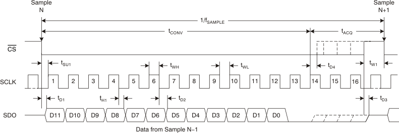
7.9 Switching Characteristics
at DVDD = 1.65 V to AVDD (unless otherwise noted); minimum and maximum values at TA = –40°C to +125°C, typical values at TA = 25°C| PARAMETER | TEST CONDITIONS(1) | MIN | TYP | MAX | UNIT | ||
|---|---|---|---|---|---|---|---|
| tCONV | Conversion time | ADS7947 (12 bit) | 13.5 | SCLK | |||
| ADS7948 (10 bit) | 10.5 | ||||||
| ADS7949 (8 bit) | 8.5 | ||||||
| tD1 | Delay time, CS low to first data (D0-15) out | DVDD = 1.8 V | 14.5 | ns | |||
| DVDD = 3 V | 12.5 | ||||||
| DVDD = 5 V | 8.5 | ||||||
| tD2(2) | Delay time, SCLK falling to SDO | DVDD = 1.8 V | 11 | ns | |||
| DVDD = 3 V | 9 | ||||||
| DVDD = 5 V | 7.1 | ||||||
| tH1 | Hold time, SCLK falling to data valid | DVDD = 1.8 V | 4 | ns | |||
| DVDD = 3 V | 3 | ||||||
| DVDD = 5 V | 2 | ||||||
| tD3 | Delay time, CS high to SDO 3-state | DVDD = 1.8 V | 15 | ns | |||
| DVDD = 3 V | 12.5 | ||||||
| DVDD = 5 V | 8.5 | ||||||
(1) 1.8-V specifications apply from 1.65 V to 2 V; 3-V specifications apply form 2.7 V to 3.6 V; 5-V specifications apply from 4.75 V to 5.25 V.
(2) With 50-pF load.
 Figure 1. Timing Diagram