SPRS710E November 2010 – March 2014 AM1802
PRODUCTION DATA.
- 1AM1802 ARM Microprocessor
- 2Revision History
-
3Device Overview
- 3.1 Device Characteristics
- 3.2 Device Compatibility
- 3.3 ARM Subsystem
- 3.4 Memory Map Summary
- 3.5 Pin Assignments
- 3.6 Pin Multiplexing Control
- 3.7
Terminal Functions
- 3.7.1 Device Reset and JTAG
- 3.7.2 High-Frequency Oscillator and PLL
- 3.7.3 Real-Time Clock and 32-kHz Oscillator
- 3.7.4 DEEPSLEEP Power Control
- 3.7.5 External Memory Interface A (EMIFA)
- 3.7.6 DDR2/mDDR Memory Controller
- 3.7.7 Serial Peripheral Interface Modules (SPI)
- 3.7.8 Boot
- 3.7.9 Universal Asynchronous Receiver/Transmitters (UART0, UART1, UART2)
- 3.7.10 Inter-Integrated Circuit Modules (I2C0)
- 3.7.11 Timers
- 3.7.12 Multichannel Audio Serial Ports (McASP)
- 3.7.13 Universal Serial Bus Modules (USB0)
- 3.7.14 Ethernet Media Access Controller (EMAC)
- 3.7.15 Multimedia Card/Secure Digital (MMC/SD)
- 3.7.16 General Purpose Input Output
- 3.7.17 Reserved and No Connect
- 3.7.18 Supply and Ground
- 3.8 Unused Pin Configurations
- 4Device Configuration
-
5Specifications
- 5.1 Absolute Maximum Ratings Over Operating Junction Temperature Range (Unless Otherwise Noted)
- 5.2 Handling Ratings
- 5.3 Recommended Operating Conditions
- 5.4 Notes on Recommended Power-On Hours (POH)
- 5.5 Electrical Characteristics Over Recommended Ranges of Supply Voltage and Operating Junction Temperature (Unless Otherwise Noted)
-
6Peripheral Information and Electrical Specifications
- 6.1 Parameter Information
- 6.2 Recommended Clock and Control Signal Transition Behavior
- 6.3 Power Supplies
- 6.4 Reset
- 6.5 Crystal Oscillator or External Clock Input
- 6.6 Clock PLLs
- 6.7 Interrupts
- 6.8 Power and Sleep Controller (PSC)
- 6.9 EDMA
- 6.10 External Memory Interface A (EMIFA)
- 6.11
DDR2/mDDR Controller
- 6.11.1 DDR2/mDDR Memory Controller Electrical Data/Timing
- 6.11.2 DDR2/mDDR Controller Register Description(s)
- 6.11.3
DDR2/mDDR Interface
- 6.11.3.1 DDR2/mDDR Interface Schematic
- 6.11.3.2 Compatible JEDEC DDR2/mDDR Devices
- 6.11.3.3 PCB Stackup
- 6.11.3.4 Placement
- 6.11.3.5 DDR2/mDDR Keep Out Region
- 6.11.3.6 Bulk Bypass Capacitors
- 6.11.3.7 High-Speed Bypass Capacitors
- 6.11.3.8 Net Classes
- 6.11.3.9 DDR2/mDDR Signal Termination
- 6.11.3.10 VREF Routing
- 6.11.3.11 DDR2/mDDR CK and ADDR_CTRL Routing
- 6.11.3.12 MDDR/DDR2 Boundary Scan Limitations
- 6.12 Memory Protection Units
- 6.13 MMC / SD / SDIO (MMCSD0)
- 6.14 Multichannel Audio Serial Port (McASP)
- 6.15 Serial Peripheral Interface Ports (SPI0, SPI1)
- 6.16 Inter-Integrated Circuit Serial Ports (I2C)
- 6.17 Universal Asynchronous Receiver/Transmitter (UART)
- 6.18 Universal Serial Bus OTG Controller (USB0) [USB2.0 OTG]
- 6.19 Ethernet Media Access Controller (EMAC)
- 6.20 Management Data Input/Output (MDIO)
- 6.21 Timers
- 6.22 Real Time Clock (RTC)
- 6.23 General-Purpose Input/Output (GPIO)
- 6.24 Emulation Logic
- 7Device and Documentation Support
- 8Mechanical Packaging and Orderable Information
Package Options
Refer to the PDF data sheet for device specific package drawings
Mechanical Data (Package|Pins)
- ZCE|361
- ZWT|361
Thermal pad, mechanical data (Package|Pins)
Orderable Information
1 AM1802 ARM Microprocessor
1.1 Features
- 300-MHzARM926EJ-S™ RISC MPU
- ARM926EJ-S Core
- 32-Bit and 16-Bit (Thumb®) Instructions
- Single-Cycle MAC
- ARM Jazelle® Technology
- Embedded ICE-RT™ for Real-Time Debug
- ARM9™ Memory Architecture
- 16KB of Instruction Cache
- 16KB of Data Cache
- 8KB of RAM (Vector Table)
- 64KB of ROM
- Enhanced Direct Memory Access Controller 3 (EDMA3):
- 2 Channel Controllers
- 3 Transfer Controllers
- 64 Independent DMA Channels
- 16 Quick DMA Channels
- Programmable Transfer Burst Size
- 128KB of On-Chip Memory
- 1.8-V or 3.3-V LVCMOS I/Os (Except for USB and DDR2 Interfaces)
- Two External Memory Interfaces:
- EMIFA
- NOR (8- or 16-Bit-Wide Data)
- NAND (8- or 16-Bit-Wide Data)
- 16-Bit SDRAM with 128-MB Address Space
- DDR2/Mobile DDR Memory Controller with one of the following:
- 16-Bit DDR2 SDRAM with 256-MB Address Space
- 16-Bit mDDR SDRAM with 256-MB Address Space
- Three Configurable 16550-Type UART Modules:
- With Modem Control Signals
- 16-Byte FIFO
- 16x or 13x Oversampling Option
- Two Serial Peripheral Interfaces (SPIs) Each with Multiple Chip Selects
- One Multimedia Card (MMC)/Secure Digital (SD) Card Interfaces with Secure Data I/O (SDIO) Interfaces
- One Master and Slave Inter-Integrated Circuit (I2C Bus™)
- USB 2.0 OTG Port with Integrated PHY (USB0)
- USB 2.0 High- and Full-Speed Client
- USB 2.0 High-, Full-, and Low-Speed Host
- End Point 0 (Control)
- End Points 1, 2, 3, 4 (Control, Bulk, Interrupt or ISOC) RX and TX
- One Multichannel Audio Serial Port (McASP):
- Transmit and Receive Clocks
- Two Clock Zones and 16 Serial Data Pins
- Supports TDM, I2S, and Similar Formats
- DIT-Capable
- FIFO Buffers for Transmit and Receive
- 10/100 Mbps Ethernet MAC (EMAC):
- IEEE 802.3 Compliant
- MII Media-Independent Interface
- RMII Reduced Media-Independent Interface
- Management Data I/O (MDIO) Module
- Real-Time Clock (RTC) with 32-kHz Oscillator and Separate Power Rail
- Three 64-Bit General-Purpose Timers (Each Configurable as Two 32-Bit Timers)
- One 64-Bit General-Purpose or Watchdog Timer (Configurable as Two 32-Bit General-Purpose Timers)
- Packages:
- 361-Ball Pb-Free Plastic Ball Grid Array (PBGA) [ZCE Suffix], 0.65-mm Ball Pitch
- 361-Ball PBGA [ZWT Suffix], 0.80-mm Ball Pitch
- Industrial Temperature
1.2 Applications
- Medical, Healthcare, and Fitness
- Building Automation
- ePOS
1.3 Description
The AM1802 ARM microprocessor is a low-power applications processor based on ARM926EJ-S.
The device enables original-equipment manufacturers (OEMs) and original-design manufacturers (ODMs) to quickly bring to market devices featuring robust operating systems support, rich user interfaces, and high processing performance life through the maximum flexibility of a fully integrated mixed processor solution.
The ARM926EJ-S is a 32-bit RISC processor core that performs 32-bit or 16-bit instructions and processes 32-bit, 16-bit, or 8-bit data. The core uses pipelining so that all parts of the processor and memory system can operate continuously.
The ARM core has a coprocessor 15 (CP15), protection module, and data and program memory management units (MMUs) with table look-aside buffers. The ARM core processor has separate 16-KB instruction and 16-KB data caches. Both are four-way associative with virtual index virtual tag (VIVT). The ARM core also has 8KB of RAM (Vector Table) and 64KB of ROM.
The peripheral set includes: a 10/100 Mbps Ethernet media access controller (EMAC) with a management data input/output (MDIO) module; one USB2.0 OTG interface; one inter-integrated circuit (I2C Bus) interface; one multichannel audio serial port (McASP) with 16 serializers and FIFO buffers; two serial peripheral interfaces (SPIs) with multiple chip selects; four 64-bit general-purpose timers each configurable (one configurable as watchdog); a configurable 16-bit host-port interface (HPI); up to 9 banks of general-purpose input/output (GPIO) pins, with each bank containing 16 pins with programmable interrupt and event generation modes, multiplexed with other peripherals; three UART interfaces (each with RTS and CTS); two external memory interfaces: an asynchronous and SDRAM external memory interface (EMIFA) for slower memories or peripherals; and a higher speed DDR2/Mobile DDR controller.
The EMAC provides an efficient interface between the device and a network. The EMAC supports both 10Base-T and 100Base-TX, or 10 Mbps and 100 Mbps in either half- or full-duplex mode. Additionally, an MDIO interface is available for PHY configuration. The EMAC supports both MII and RMII interfaces.
The rich peripheral set provides the ability to control external peripheral devices and communicate with external processors. For details on each of the peripherals, see the related sections in this document and the associated peripheral reference guides.
The device has a complete set of development tools for the ARM processor. These tools include C compilers, and scheduling, and a Windows® debugger interface for visibility into source code execution.
Device Information
| PART NUMBER | PACKAGE | BODY SIZE |
|---|---|---|
| AM1802ZWT | NFBGA (361) | 16,00 mm x 16,00 mm |
| AM1802ZCE | NFBGA (361) | 13,00 mm x 13,00 mm |
1.4 Functional Block Diagram
Figure 1-1 shows the functional block diagram of the device.
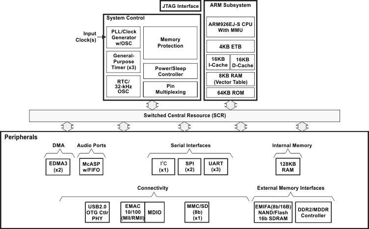 Figure 1-1 Functional Block Diagram