SPRS658F February 2010 – March 2014 AM1806
PRODUCTION DATA.
- 1 AM1806 ARM Microprocessor
- 2Revision History
-
3Device Overview
- 3.1 Device Characteristics
- 3.2 Device Compatibility
- 3.3 ARM Subsystem
- 3.4 Memory Map Summary
- 3.5 Pin Assignments
- 3.6 Pin Multiplexing Control
- 3.7
Terminal Functions
- 3.7.1 Device Reset and JTAG
- 3.7.2 High-Frequency Oscillator and PLL
- 3.7.3 Real-Time Clock and 32-kHz Oscillator
- 3.7.4 DEEPSLEEP Power Control
- 3.7.5 External Memory Interface A (EMIFA)
- 3.7.6 DDR2/mDDR Memory Controller
- 3.7.7 Serial Peripheral Interface Modules (SPI)
- 3.7.8 Programmable Real-Time Unit (PRU)
- 3.7.9 Enhanced Capture/Auxiliary PWM Modules (eCAP0)
- 3.7.10 Enhanced Pulse Width Modulators (eHRPWM)
- 3.7.11 Boot
- 3.7.12 Universal Asynchronous Receiver/Transmitters (UART0, UART1, UART2)
- 3.7.13 Inter-Integrated Circuit Modules(I2C0, I2C1)
- 3.7.14 Timers
- 3.7.15 Multichannel Audio Serial Ports (McASP)
- 3.7.16 Multichannel Buffered Serial Ports (McBSP)
- 3.7.17 Universal Serial Bus Modules (USB0)
- 3.7.18 Multimedia Card/Secure Digital (MMC/SD)
- 3.7.19 Liquid Crystal Display Controller(LCD)
- 3.7.20 Universal Host-Port Interface (UHPI)
- 3.7.21 Universal Parallel Port (uPP)
- 3.7.22 Video Port Interface (VPIF)
- 3.7.23 General Purpose Input Output
- 3.7.24 Reserved and No Connect
- 3.7.25 Supply and Ground
- 3.8 Unused Pin Configurations
- 4Device Configuration
-
5Specifications
- 5.1 Absolute Maximum Ratings Over Operating Junction Temperature Range (Unless Otherwise Noted)
- 5.2 Handling Ratings
- 5.3 Recommended Operating Conditions
- 5.4 Notes on Recommended Power-On Hours (POH)
- 5.5 Electrical Characteristics Over Recommended Ranges of Supply Voltage and Operating Junction Temperature (Unless Otherwise Noted)
-
6Peripheral Information and Electrical Specifications
- 6.1 Parameter Information
- 6.2 Recommended Clock and Control Signal Transition Behavior
- 6.3 Power Supplies
- 6.4 Reset
- 6.5 Crystal Oscillator or External Clock Input
- 6.6 Clock PLLs
- 6.7 Interrupts
- 6.8 Power and Sleep Controller (PSC)
- 6.9 EDMA
- 6.10 External Memory Interface A (EMIFA)
- 6.11
DDR2/mDDR Memory Controller
- 6.11.1 DDR2/mDDR Memory Controller Electrical Data/Timing
- 6.11.2 DDR2/mDDR Controller Register Description(s)
- 6.11.3
DDR2/mDDR Interface
- 6.11.3.1 DDR2/mDDR Interface Schematic
- 6.11.3.2 Compatible JEDEC DDR2/mDDR Devices
- 6.11.3.3 PCB Stackup
- 6.11.3.4 Placement
- 6.11.3.5 DDR2/mDDR Keep Out Region
- 6.11.3.6 Bulk Bypass Capacitors
- 6.11.3.7 High-Speed Bypass Capacitors
- 6.11.3.8 Net Classes
- 6.11.3.9 DDR2/mDDR Signal Termination
- 6.11.3.10 VREF Routing
- 6.11.3.11 DDR2/mDDR CK and ADDR_CTRL Routing
- 6.11.3.12 MDDR/DDR2 Boundary Scan Limitations
- 6.12 Memory Protection Units
- 6.13 MMC / SD / SDIO (MMCSD0, MMCSD1)
- 6.14 Multichannel Audio Serial Port (McASP)
- 6.15 Multichannel Buffered Serial Port (McBSP)
- 6.16 Serial Peripheral Interface Ports (SPI0, SPI1)
- 6.17 Inter-Integrated Circuit Serial Ports (I2C)
- 6.18 Universal Asynchronous Receiver/Transmitter (UART)
- 6.19 Universal Serial Bus OTG Controller (USB0) [USB2.0 OTG]
- 6.20 LCD Controller (LCDC)
- 6.21 Host-Port Interface (UHPI)
- 6.22 Universal Parallel Port (uPP)
- 6.23 Video Port Interface (VPIF)
- 6.24 Enhanced Capture (eCAP) Peripheral
- 6.25 Enhanced High-Resolution Pulse-Width Modulator (eHRPWM)
- 6.26 Timers
- 6.27 Real Time Clock (RTC)
- 6.28 General-Purpose Input/Output (GPIO)
- 6.29 Programmable Real-Time Unit Subsystem (PRUSS)
- 6.30 Emulation Logic
- 7Device and Documentation Support
- 8Mechanical Packaging and Orderable Information
Package Options
Refer to the PDF data sheet for device specific package drawings
Mechanical Data (Package|Pins)
- ZCE|361
- ZWT|361
Thermal pad, mechanical data (Package|Pins)
Orderable Information
7 Device and Documentation Support
7.1 Device Support
7.1.1 Development Support
TI offers an extensive line of development tools for the device platform, including tools to evaluate the performance of the processors, generate code, develop algorithm implementations, and fully integrate and debug software and hardware modules. The tool's support documentation is electronically available within the Code Composer Studio™ Integrated Development Environment (IDE).
The following products support development of the device applications:
Software Development Tools:
Code Composer Studio™ Integrated Development Environment (IDE): including Editor
C/C++/Assembly Code Generation, and Debug plus additional development tools
Hardware Development Tools:
Extended Development System (XDS™) Emulator
For a complete listing of development-support tools for the device, visit the Texas Instruments web site on the Worldwide Web at www.ti.com uniform resource locator (URL). For information on pricing and availability, contact the nearest TI field sales office or authorized distributor.
7.1.2 Device and Development-Support Tool Nomenclature
To designate the stages in the product development cycle, TI assigns prefixes to the part numbers of all AM1xxx processors and support tools. Each commercial AM1xxx platform member has one of three prefixes: X, P, or null (no prefix). Texas Instruments recommends two of three possible prefix designators for its support tools: TMDX and TMDS. These prefixes represent evolutionary stages of product development from engineering prototypes (TMDX) through fully qualified production devices/tools (TMDS).
Device development evolutionary flow:
-
X Experimental device that is not necessarily representative of the final device's electrical specifications.
-
P Final silicon die that conforms to the device's electrical specifications but has not completed quality and reliability verification.
-
NULL Fully-qualified production device.
Support tool development evolutionary flow:
-
TMDX Development-support product that has not yet completed Texas Instruments internal qualification testing.
-
TMDS Fully qualified development-support product.
X and P devices and TMDX development-support tools are shipped against the following disclaimer:
"Developmental product is intended for internal evaluation purposes."
NULL devices and TMDS development-support tools have been characterized fully, and the quality and reliability of the device have been demonstrated fully. TI's standard warranty applies.
Predictions show that prototype devices (X or P) have a greater failure rate than the standard production devices. Texas Instruments recommends that these devices not be used in any production system because their expected end-use failure rate still is undefined. Only qualified production devices are to be used.
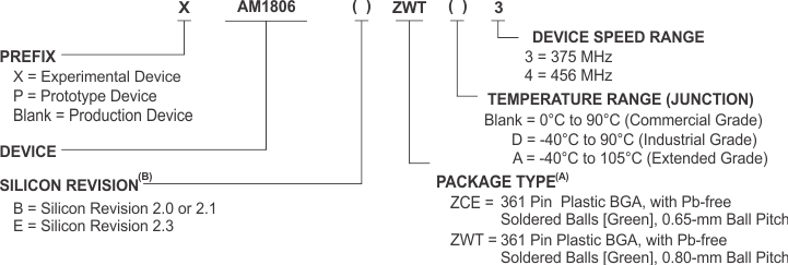
Figure 7-1 provides a legend for reading the complete device.
7.2 Documentation Support
The following documents describe the device. Copies of these documents are available on the Internet at www.ti.com. Tip: Enter the literature number in the search box provided at www.ti.com.
7.3 Community Resources
The following links connect to TI community resources. Linked contents are provided "AS IS" by the respective contributors. They do not constitute TI specifications and do not necessarily reflect TI's views; see TI's Terms of Use.
-
TI E2E™ Online Community TI's Engineer-to-Engineer (E2E) Community. Created to foster collaboration among engineers. At e2e.ti.com, you can ask questions, share knowledge, explore ideas and help solve problems with fellow engineers.
-
TI Embedded Processors Wiki Texas Instruments Embedded Processors Wiki. Established to help developers get started with Embedded Processors from Texas Instruments and to foster innovation and growth of general knowledge about the hardware and software surrounding these devices.
7.4 Trademarks
E2E is a trademark of Texas Instruments.
ARM926EJ-S is a trademark of ARM Ltd.
Windows is a registered trademark of Microsoft.
I2C Bus is a trademark of Phillips.
All other trademarks are the property of their respective owners.
7.5 Electrostatic Discharge Caution

This integrated circuit can be damaged by ESD. Texas Instruments recommends that all integrated circuits be handled with appropriate precautions. Failure to observe proper handling and installation procedures can cause damage.
ESD damage can range from subtle performance degradation to complete device failure. Precision integrated circuits may be more susceptible to damage because very small parametric changes could cause the device not to meet its published specifications.
7.6 Glossary
SLYZ022 — TI Glossary.
This glossary lists and explains terms, acronyms and definitions.