SLAS836 March 2014 AMC7832
PRODUCTION DATA.
- 1 Features
- 2 Applications
- 3 Description
- 4 Power Amp Biasing Diagram
- 5 Revision History
- 6 Terminal Configuration and Functions
-
7 Specifications
- 7.1 Absolute Maximum Ratings
- 7.2 Handling Ratings
- 7.3 Recommended Operating Conditions
- 7.4 Thermal Information
- 7.5 Electrical Characteristics
- 7.6 Timing Requirements - Serial Interface
- 7.7 Typical Characteristics: DAC
- 7.8 Typical Characteristics: ADC
- 7.9 Typical Characteristics: Reference
- 7.10 Typical Characteristics: Temperature Sensor
-
8 Detailed Description
- 8.1 Overview
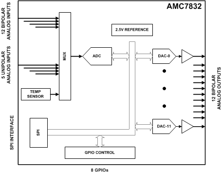
- 8.2 Functional Block Diagram
- 8.3 Feature Description
- 8.4 Programming
- 8.5
Register Map
- 8.5.1 Interface Configuration: Address 0x00 - 0x02
- 8.5.2 Device Identification: Address 0x03 - 0x0D
- 8.5.3 Register Update (Buffered Registers): Address 0x0F
- 8.5.4 General Device Configuration: Address 0x10 - 0x17
- 8.5.5 DAC Clear And ALARMOUT Source Select: Address 0x1A - 0x1D
- 8.5.6 DAC Range: Address 0x1E
- 8.5.7 ADC Data: Address 0x20 - 0x41
- 8.5.8 DAC Data: Address 0x50 - 0x67
- 8.5.9 Status Registers: Address 0x70 - 0x72
- 8.5.10 Temperature And GPIO Data: Address 0x78 - 0x7A
- 8.5.11 Out-Of-Range ADC Thresholds: Address 0x80 - 0x93
- 8.5.12 Hysteresis: Address 0xA0 - 0xA5
- 8.5.13 Power-Down Registers: Address 0xB0 - 0xB3
- 8.5.14 ADC Trigger: Address 0xC0
- 9 Applications and Implementation
- 10Power Supply Recommendations
- 11Layout
- 12Device and Documentation Support
- 13Mechanical, Packaging, and Orderable Information
Package Options
Mechanical Data (Package|Pins)
- PAP|64
Thermal pad, mechanical data (Package|Pins)
- PAP|64
Orderable Information
1 Features
- Twelve Monotonic 12-Bit DACs
- Selectable Ranges: 0 to +5-V, 0 to +10-V and
-10 to 0-V - High Current Drive Capability: up to ±15-mA
- Selectable Clamp Voltage
- One 12-Bit SAR ADC
- 17 External Analog Inputs
- 12 Bipolar Inputs: -12.5-V to +12.5-V Range
- 5 High Precision Inputs: 0 to +5-V Range
- Programmable Out-of-Range Alarms
- Internal +2.5-V Reference
- Internal Temperature Sensor
- -40°C to +125°C Operation
- ±2.5°C Accuracy
- Eight General Purpose I/O Ports (GPIOs)
- Low Power SPI Compatible Serial Interface
- 4-Wire Mode, +1.8-V to +5.5-V Operation
- Operating Temperature Range: -40°C to +125°C
- Available in 64-Terminal HTQFP PowerPAD Package
2 Applications
- Communications Infrastructure:
- Cellular Base Stations
- Microwave Backhaul
- Optical Networks
- General Purpose Monitor & Control
- Data Acquisition Systems
3 Description
The AMC7832 is a highly integrated, low-power, analog monitoring and control solution that includes a 17-channel, 12-bit analog-to-digital converter (ADC) with programmable alarms, twelve 12-bit digital-to-analog converters (DACs) with output ranges of either 0 to +5-V, 0 to +10-V or -10 to 0-V, eight GPIOs, internal reference and a local temperature sensor channel. The AMC7832 high level of integration significantly reduces component count and simplifies closed-loop system designs.
The AMC7832 is ideal for multichannel applications where board space, size, and low power are critical.
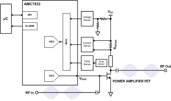
The AMC7832’s low power, high-integration and wide operating temperature range make it an ideal all-in-one, low-cost, bias control circuit for the power amplifiers (PA) found in multi-channel RF communication systems. The flexible DAC output ranges allow the device to be used as a biasing solution for a large variety of transistor technologies such as LDMOS, GaAs and GaN. The AMC7832 feature set is similarly beneficial in general purpose monitor and control systems.
For applications that require a different channel count, additional features, or converter resolutions, Texas Instruments offers a complete family of Analog Monitor and Control (AMC) products. Visit http://www.ti.com/amc for more information.
Device Information
| ORDER NUMBER | PACKAGE | BODY SIZE |
|---|---|---|
| AMC7832IPAP | HTQFP (64) | 10mm x 10mm |
4 Power Amp Biasing Diagram
Functional Diagram