SLUSCE2D April   2016  – January 2019

PRODUCTION DATA.  

  1. Features
  2. Applications
  3. Description
    1.     Device Images
      1.      Simplified Schematic
  4. Revision History
  5. Device Comparison
  6. Pin Configuration and Functions
    1.     Pin Functions
  7. Specifications
    1. 7.1 Absolute Maximum Ratings
    2. 7.2 ESD Ratings
    3. 7.3 Recommended Operating Conditions
    4. 7.4 Thermal Information
    5. 7.5 Electrical Characteristics
    6. 7.6 Timing Requirements
    7. 7.7 Typical Operational Characteristics (Protection Circuits Waveforms)
  8. Detailed Description
    1. 8.1 Overview
    2. 8.2 Functional Block Diagram
    3. 8.3 Feature Description
      1. 8.3.1 Power-Down or Undervoltage Lockout (UVLO)
      2. 8.3.2 Power-up
      3. 8.3.3 Sleep Mode
      4. 8.3.4 New Charge Cycle
      5. 8.3.5 Overvoltage-Protection (OVP) – Continuously Monitored
      6. 8.3.6 CHG Terminal Indication
    4. 8.4 Device Functional Modes
      1. 8.4.1  CHG LED Pull-up Source
      2. 8.4.2  IN-DPM (VIN-DPM or IN-DPM)
      3. 8.4.3  OUT
      4. 8.4.4  ISET
      5. 8.4.5  TS
      6. 8.4.6  Termination and Timer Disable Mode (TTDM) - TS Terminal High
      7. 8.4.7  Timers
      8. 8.4.8  Termination
      9. 8.4.9  Battery Detect Routine
      10. 8.4.10 Refresh Threshold
      11. 8.4.11 Starting a Charge on a Full Battery
  9. Application and Implementation
    1. 9.1 Application Information
    2. 9.2 Typical Application
      1. 9.2.1 Design Requirements
      2. 9.2.2 Detailed Design Procedure
        1. 9.2.2.1 Calculations
          1. 9.2.2.1.1 Program the Fast Charge Current, ISET:
          2. 9.2.2.1.2 Pre-Charge and Termination Current Thresholds, ITERM, and PRE-CHG
          3. 9.2.2.1.3 TS Function
          4. 9.2.2.1.4 CHG
        2. 9.2.2.2 Selecting In and Out Terminal Capacitors
      3. 9.2.3 Application Curves
  10. 10Power Supply Recommendations
  11. 11Layout
    1. 11.1 Layout Guidelines
    2. 11.2 Layout Example
    3. 11.3 Thermal Considerations
      1. 11.3.1 Leakage Current Effects on Battery Capacity
  12. 12Device and Documentation Support
    1. 12.1 Receiving Notification of Documentation Updates
    2. 12.2 Community Resources
    3. 12.3 Trademarks
    4. 12.4 Electrostatic Discharge Caution
    5. 12.5 Glossary
  13. 13Mechanical, Packaging, and Orderable Information

Package Options

Mechanical Data (Package|Pins)
Thermal pad, mechanical data (Package|Pins)
Orderable Information

Application Curves

SETUP: bq21040 typical applications schematic; VIN = 5V, VBAT = 3.6V (unless otherwise indicated)
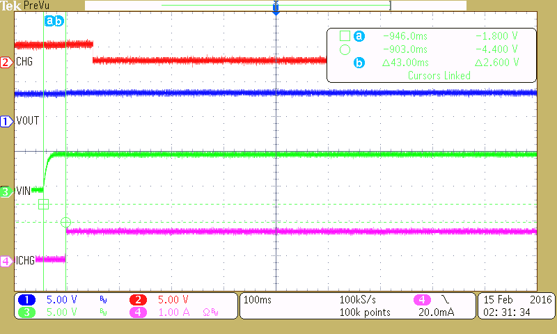
bq21040 Power_up_Timing_SLUSCE2.png
Figure 11. Power-Up Timing  
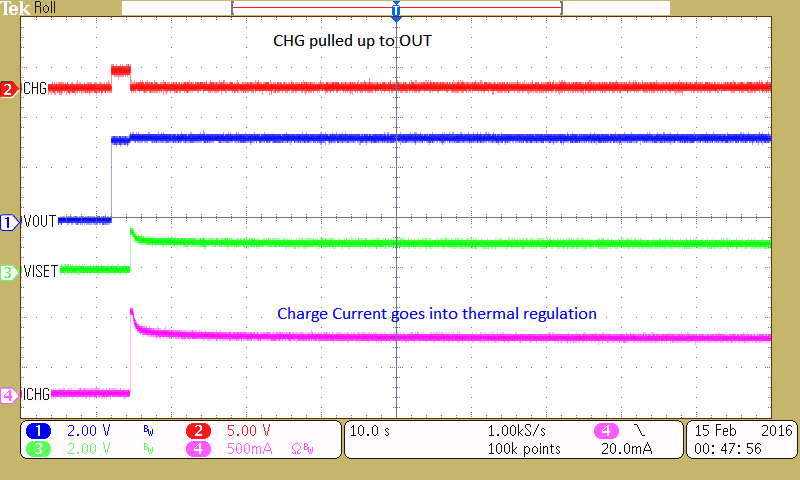
bq21040 Start_up_in_thermal_regulation_SLUSCE2.png
Figure 13. Start-Up in Thermal Regulation
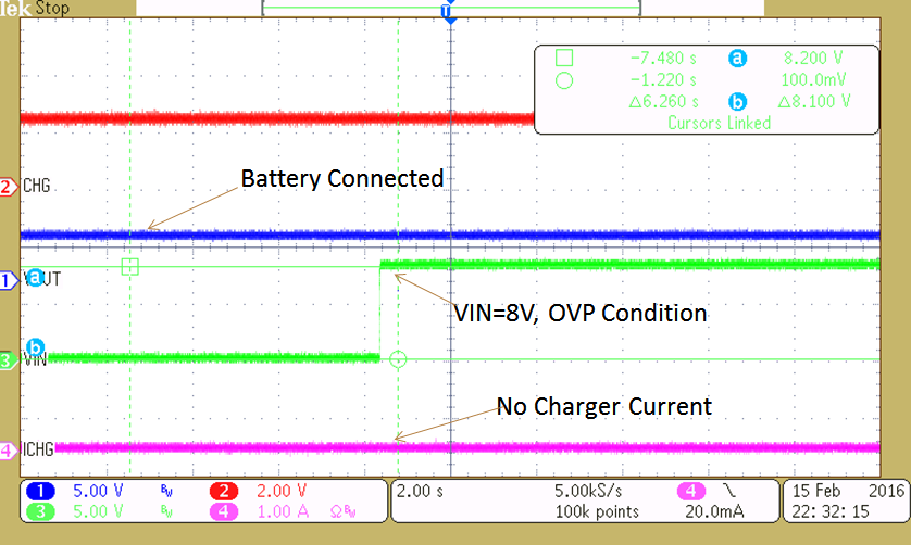
bq21040 OVP_8V_Adaptor_Hot_Plug_SLUSCE2.png
Figure 15. OVP 8-V Adaptor — Hot Plug
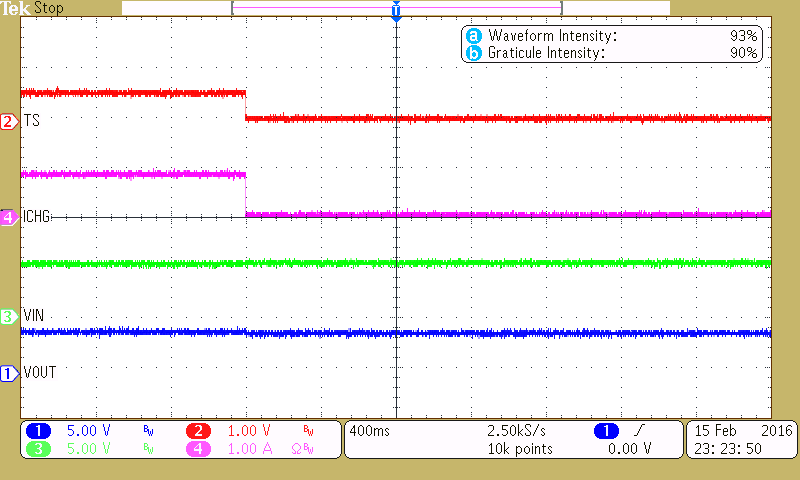
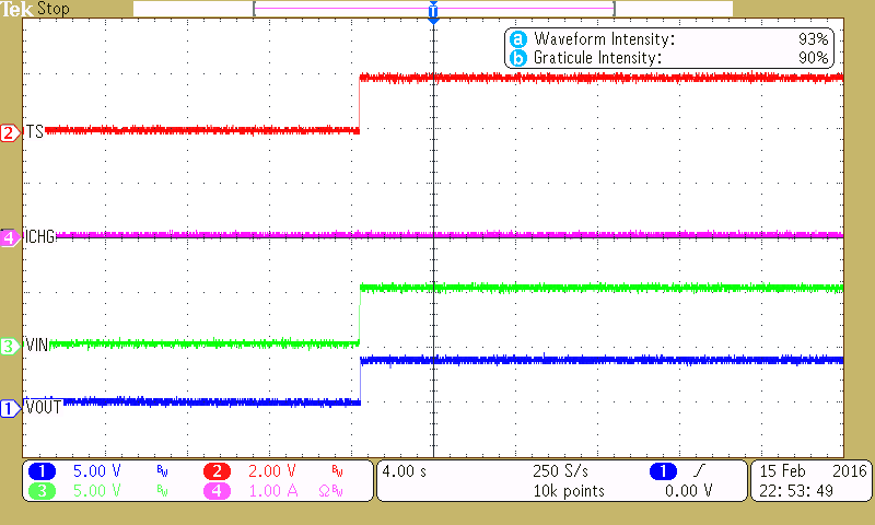
bq21040 TS_Enable_and_Disable_SLUSCE2.png
10-kΩ resistor from TS to GND. 10 kΩ is shorted to disable the IC
.
Figure 17. TS Enable and Disable  
bq21040 Battery_Removal_GND_Removed_1st_42_Ohms_Load_SLUSCE2.png
Figure 19. Battery Removal – GND Removed 1st, 42-Ω Load  
bq21040 Battery_Removal_with_fixed_TS _0.5V_SLUSCE2.png
Continuous battery detection when not in TTDM
Figure 21. Battery Removal With Fixed TS = 0.5 V  
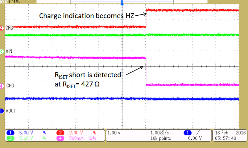
bq21040 ISET_Shorted_During_Normal_Operation_SLUSCE2.png
CH4: IOUT (1A/Div)
Figure 23. ISET Shorted During Normal Operation  
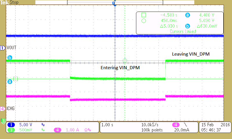
bq21040 VIN_DPM _Adaptor_Current_Limits _Vin_Regulated_SLUSCE2.png
CH4: IOUT (0.2A/Div)
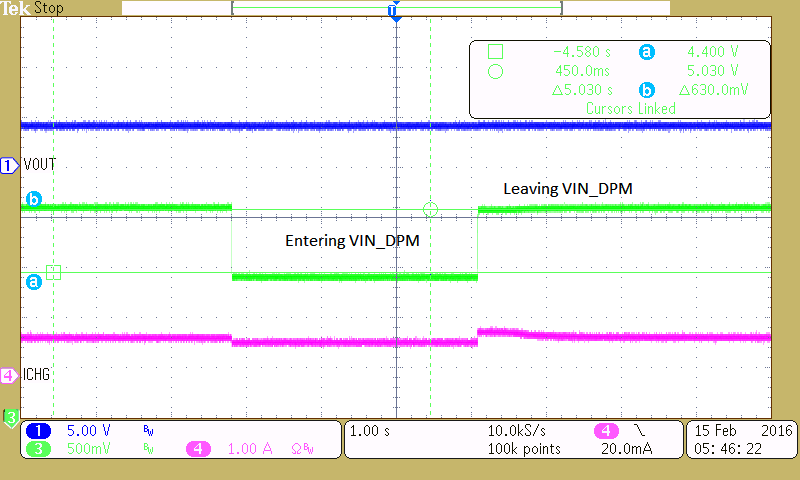
Figure 25. DPM – Adaptor Current Limits – VIN Regulated  
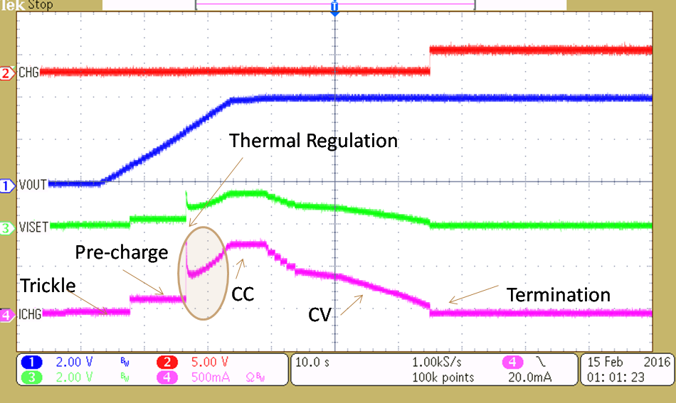
bq21040 charge_cycle_with_Thermal_Reg_SLUSCE2.png
The IC temperature rises to 125°C and enters thermal regulation. Charge current is reduced to regulate the IC at 125°C. VIN is reduced, the IC temperature drops, the charge current returns to the programmed value
.
Figure 27. Charge Cycle With Thermal Regulation
bq21040 Power_up_Timing _No_Battery_or_Load-in-TTDM_SLUSCE2.png
Figure 12. Power-Up Timing – No Battery or Load in TTDM
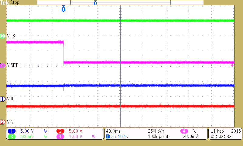
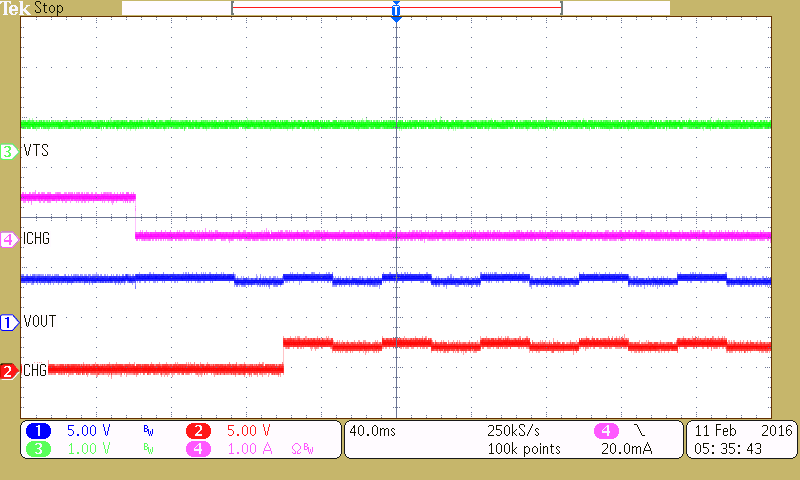
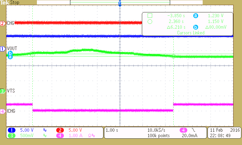
bq21040 TS_entering_and_leaving_Cold_Temp_SLUSCE2.png
Figure 14. TS Entering and Leaving Cold Temperature
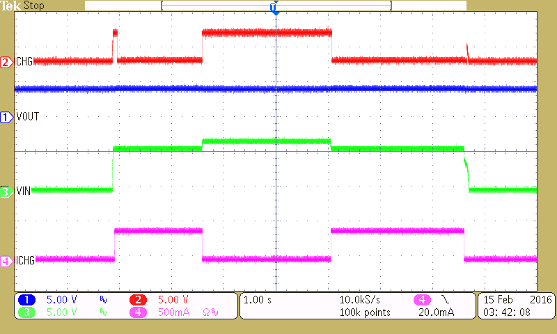
bq21040 OVP_from_Normal_Power-up_VIN_0V_to_6V_to_7V_to_6V_to_0V_to_SLUSCE2.png
Figure 16. OVP From Normal Power-Up
Operation – VIN 0 V → 6 V → 7 V → 6 V→ 0 V
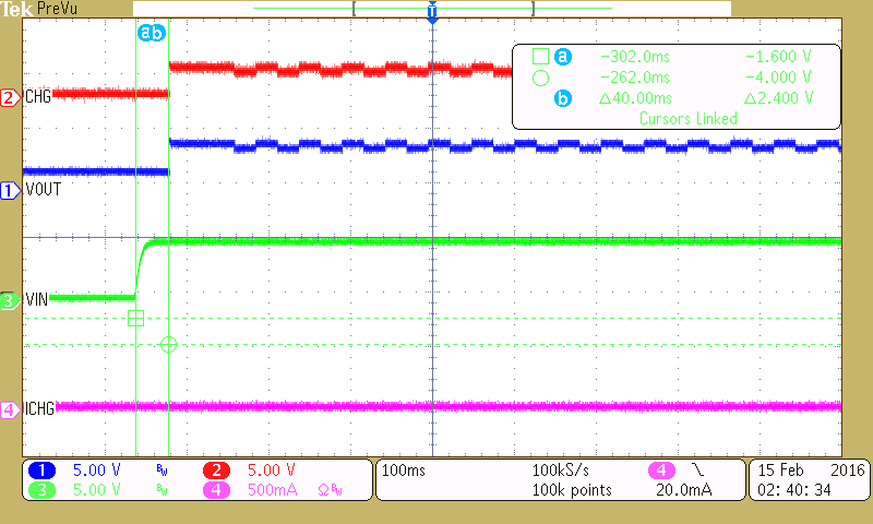
bq21040 Power_up_Timing_No_Battery_No_Load_BATT_DET_SLUSCE2.png
Fixed 10kΩ resistor, between TS and GND.
Figure 18. Power-Up Timing with No Battery and No Load – Battery Detection
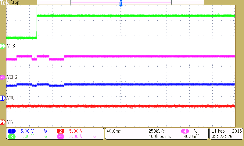
bq21040 Battery_Removal_with_OUT_and_TS_disconnect_1st_with_100_Phms_Load_SLUSCE2.png
Figure 20. Battery Removal With OUT and
TS Disconnect 1st, With 100-Ω Load
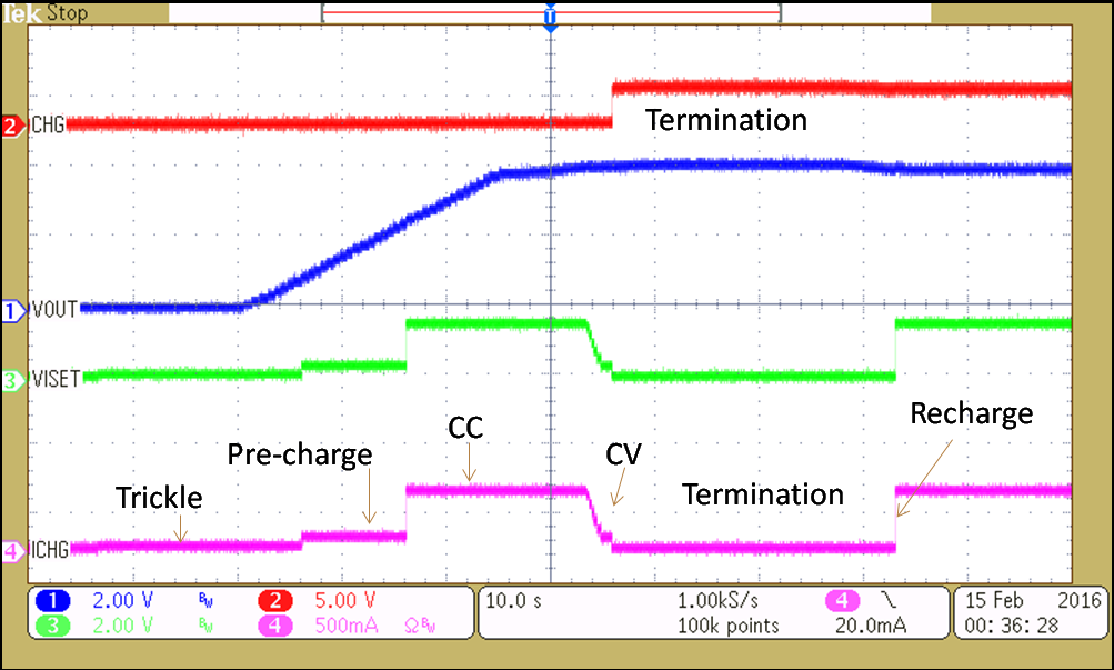
bq21040 Battery_Charge_Profile_SLUSCE2.png
CH4: IOUT (1A/Div)
Battery voltage swept from 0V to 4.25V to 3.9V.
Figure 22. Battery Charge Profile  
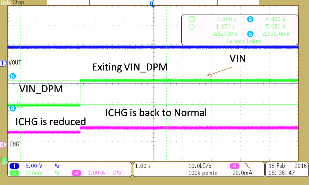
bq21040 Charge_Current_Reduced_During_VIN_DPM_Mode_SLUSCE2.png
CH4: IOUT (0.2A/Div)
Figure 24. ISET Shorted Prior to USB Power-up  
bq21040 DPM _USB_Current_Limits _Vin_Regulated_to_4.4V_SLUSCE2.png
Figure 26. DPM – USB Current Limits – VIN Regulated to 4.4 V
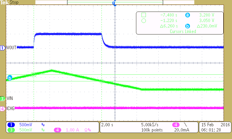
bq21040 Entering_and_Exiting_UVLO_SLUSCE2.png
VIN swept from 5 V to 3.9 V to 5 V VBAT = 4 V
Figure 28. Entering and Exiting UVLO