SLUSCE2D April   2016  – January 2019

PRODUCTION DATA.  

  1. Features
  2. Applications
  3. Description
    1.     Device Images
      1.      Simplified Schematic
  4. Revision History
  5. Device Comparison
  6. Pin Configuration and Functions
    1.     Pin Functions
  7. Specifications
    1. 7.1 Absolute Maximum Ratings
    2. 7.2 ESD Ratings
    3. 7.3 Recommended Operating Conditions
    4. 7.4 Thermal Information
    5. 7.5 Electrical Characteristics
    6. 7.6 Timing Requirements
    7. 7.7 Typical Operational Characteristics (Protection Circuits Waveforms)
  8. Detailed Description
    1. 8.1 Overview
    2. 8.2 Functional Block Diagram
    3. 8.3 Feature Description
      1. 8.3.1 Power-Down or Undervoltage Lockout (UVLO)
      2. 8.3.2 Power-up
      3. 8.3.3 Sleep Mode
      4. 8.3.4 New Charge Cycle
      5. 8.3.5 Overvoltage-Protection (OVP) – Continuously Monitored
      6. 8.3.6 CHG Terminal Indication
    4. 8.4 Device Functional Modes
      1. 8.4.1  CHG LED Pull-up Source
      2. 8.4.2  IN-DPM (VIN-DPM or IN-DPM)
      3. 8.4.3  OUT
      4. 8.4.4  ISET
      5. 8.4.5  TS
      6. 8.4.6  Termination and Timer Disable Mode (TTDM) - TS Terminal High
      7. 8.4.7  Timers
      8. 8.4.8  Termination
      9. 8.4.9  Battery Detect Routine
      10. 8.4.10 Refresh Threshold
      11. 8.4.11 Starting a Charge on a Full Battery
  9. Application and Implementation
    1. 9.1 Application Information
    2. 9.2 Typical Application
      1. 9.2.1 Design Requirements
      2. 9.2.2 Detailed Design Procedure
        1. 9.2.2.1 Calculations
          1. 9.2.2.1.1 Program the Fast Charge Current, ISET:
          2. 9.2.2.1.2 Pre-Charge and Termination Current Thresholds, ITERM, and PRE-CHG
          3. 9.2.2.1.3 TS Function
          4. 9.2.2.1.4 CHG
        2. 9.2.2.2 Selecting In and Out Terminal Capacitors
      3. 9.2.3 Application Curves
  10. 10Power Supply Recommendations
  11. 11Layout
    1. 11.1 Layout Guidelines
    2. 11.2 Layout Example
    3. 11.3 Thermal Considerations
      1. 11.3.1 Leakage Current Effects on Battery Capacity
  12. 12Device and Documentation Support
    1. 12.1 Receiving Notification of Documentation Updates
    2. 12.2 Community Resources
    3. 12.3 Trademarks
    4. 12.4 Electrostatic Discharge Caution
    5. 12.5 Glossary
  13. 13Mechanical, Packaging, and Orderable Information

Package Options

Mechanical Data (Package|Pins)
Thermal pad, mechanical data (Package|Pins)
Orderable Information

ISET

An external resistor is used to Program the Output Current (50 to 800 mA) and can be used as a current monitor.

Equation 1. RISET = KISET / IOUT

where

  • IOUT is the desired fast charge current;
  • KISET is a gain factor found in the electrical specification

For greater accuracy at lower currents, part of the sense FET is disabled to give better resolution. Figure 1 shows the transition from low current to higher current. Going from higher currents to low currents, there is hysteresis and the transition occurs around 0.15 A.

The ISET resistor is short protected and will detect a resistance lower than ≉340 Ω. The detection requires at least 80mA of output current. If a “short” is detected, then the IC will latch off and can only be reset by cycling the power. The OUT current is internally clamped to a maximum current between 1.05 A and 1.4 A and is independent of the ISET short detection circuitry, as shown in Figure 8. Also, see Figure 23 and Figure 24.
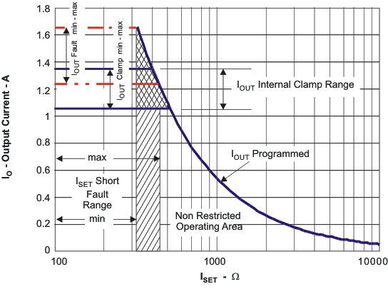
bq21040 clamp2_io_lus940.gifFigure 8. Programmed/Clamped Out Current