SLUSB97A October 2012 – December 2014
PRODUCTION DATA.
- 1 Features
- 2 Applications
- 3 Description
- 4 Revision History
- 5 Description (Continued)
- 6 Pin Configuration and Functions
- 7 Specifications
-
8 Detailed Description
- 8.1 Overview
- 8.2 Functional Block Diagram
- 8.3
Feature Description
- 8.3.1 Device Power Up
- 8.3.2 Power Path Management
- 8.3.3 Battery Charging Management
- 8.3.4 Status Outputs (STAT and INT)
- 8.3.5 Protections
- 8.3.6 Serial Interface
- 8.4 Device Functional Modes
- 8.5
Register Map
- 8.5.1
I2C Registers
- 8.5.1.1 Input Source Control Register REG00 (reset = 00110000, or 30)
- 8.5.1.2 Power-On Configuration Register REG01 (reset = 00011011, or 1B)
- 8.5.1.3 Charge Current Control Register REG02 (reset = 01100000, or 60)
- 8.5.1.4 Pre-Charge/Termination Current Control Register REG03 (reset = 00010001, or 11)
- 8.5.1.5 Charge Voltage Control Register REG04 (reset = 10110010, or B2)
- 8.5.1.6 Charge Termination/Timer Control Register REG05 (reset = 10011010, or 9A)
- 8.5.1.7 Thermal Regulation Control Register REG06 (reset = 00000011, or 03)
- 8.5.1.8 Misc Operation Control Register REG07 (reset = 01001011, or 4B)
- 8.5.1.9 System Status Register REG08
- 8.5.1.10 Fault Register REG09
- 8.5.1.11 Vender / Part / Revision Status Register REG0A (reset = 00100011, or 23)
- 8.5.1
I2C Registers
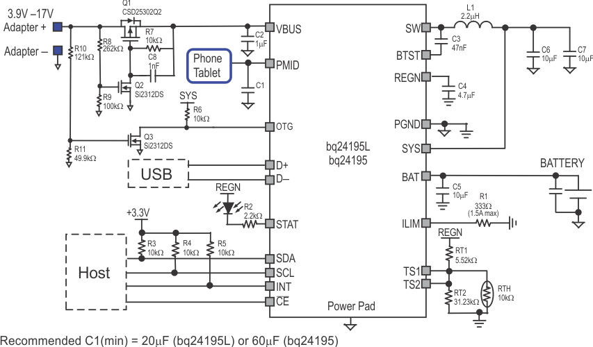
- 9 Application and Implementation
- 10Power Supply Recommendations
- 11Layout
- 12Device and Documentation Support
- 13Mechanical, Packaging, and Orderable Information
Package Options
Mechanical Data (Package|Pins)
- RGE|24
Thermal pad, mechanical data (Package|Pins)
- RGE|24
Orderable Information
1 Features
- High Efficiency Switch Mode Charger
- 2.5-A (bq24195L) or 4.5-A (bq24195) Fast Charging
- 92% Charge Efficiency at 2 A, 90% at 4 A
- Synchronous Boost Converter in Battery Boost Mode
- 5.1 V at 1 A (bq24195L) or 5.1 V at 2.1 A (bq24195)
- 94% 5.1-V Boost Efficiency at 1 A,
91% at 2.1 A
- Highest Battery Discharge Efficiency with 12-mΩ Battery Discharge MOSFET up to 9-A Discharge Current
- Single Input USB-compliant/Adapter Charger
- USB Host or Charging Port D+/D- Detection Compatible to USB Battery Charger Spec 1.2
- Input Voltage and Current Limit Supports USB2.0 and USB3.0
- Input Current Limit: 100 mA, 150 mA, 500 mA, 900 mA, 1.2 A, 1.5 A, 2 A and 3 A
- 3.9-V to 17-V Input Operating Voltage Range
- Support All Kinds of Adapter with Input Voltage DPM Regulation
- Narrow VDC (NVDC) Power Path Management
- Instant-on Works with No Battery or Deeply Discharged Battery
- Ideal Diode Operation in Battery Supplement Mode
- 1.5-MHz Switching Frequency for Low Profile Inductor
- Autonomous Battery Charging with or without Host Management
- Battery Charge Enable
- Battery Charge Preconditioning
- Charge Termination and Recharge
- High Accuracy (0°C to 125°C)
- ±0.5% Charge Voltage Regulation
- ±7% Charge Current Regulation
- ±7.5% Input Current Regulation
- ±2% Output Regulation in Boost Mode
- High Integration
- Power Path Management
- Synchronous Switching MOSFETs
- Integrated Current Sensing
- Bootstrap Diode
- Internal Loop Compensation
- Safety
- Battery Temperature Sensing and Charging Safety Timer
- Thermal Regulation and Thermal Shutdown
- Input System Over-Voltage Protection
- MOSFET Over-Current Protection
- Charge Status Outputs for LED or Host Processor
- Low Battery Leakage Current and Support Shipping Mode
- 4.00 mm x 4.00 mm QFN-24 Package
2 Applications
- Power Bank for Smartphone, Tablet
- Tablet PC and Smart Phone
- Portable Audio Speaker
- Portable Media Players
- Internet Devices
3 Description
The bq24195L, bq24195 are highly-integrated switch-mode battery charge management and system power path management devices for single cell Li-Ion and Li-polymer battery in a wide range of power bank, tablet and other portable devices.
Device Information(1)
| PART NUMBER | PACKAGE | BODY SIZE (NOM) |
|---|---|---|
| bq24195 | VQFN (24) | 4.00 mm x 4.00 mm |
| bq24195L |
- For all available packages, see the orderable addendum at the end of the datasheet.
4 Revision History
Changes from * Revision (October 2012) to A Revision
- Added Handling Rating table, Feature Description section, Device Functional Modes, Application and Implementation section, Power Supply Recommendations section, Layout section, Device and Documentation Support section, and Mechanical, Packaging, and Orderable Information section. Go
- Changed VSLEEPZ, VBAT_DPL_HY, VBATGD , ICHG_20pct, VSHORT, IADPT_DPM, KILIM, VBTST_REFRESH in Electrical CharacteristicsGo
- Added –40°C to 85° to IBAT Test ConditionGo
- Added REG00[6:3] = 0110 (4.36 V) or 1011 (4.76 V) to VINDPM_REG_ACC Test ConditionsGo
- Added a MIN value of 435 to KILIMGo
- Deleted TJunction_REG MIN and MAXGo
- Changed VOTG_ILIM to IOTG_ILIMGo
- Changed Functional Block DiagramGo
- Changed Charging Current in Table 3Go
- Changed REG09[5:4] to REG08[5:4] in Charging Termination sectionGo
- Changed Charging Safety Timer descriptionGo
- Changed Host Mode and Default Mode descriptionGo
- Changed Charge Current Control Register REG02 Bit 0 description and noteGo