SLUSB98A October 2012 – December 2014
PRODUCTION DATA.
- 1 Features
- 2 Applications
- 3 Description
- 4 Revision History
- 5 Description (Continued)
- 6 Pin Configuration and Functions
- 7 Specifications
-
8 Detailed Description
- 8.1 Overview
- 8.2 Functional Block Diagram
- 8.3
Feature Description
- 8.3.1 Device Power Up
- 8.3.2 Power Path Management
- 8.3.3 Battery Charging Management
- 8.3.4 Status Outputs (PG, STAT, and INT)
- 8.3.5 Protections
- 8.3.6 Serial Interface
- 8.4 Device Functional Modes
- 8.5
Register Map
- 8.5.1
I2C Registers
- 8.5.1.1 Input Source Control Register REG00 (reset = 00110000, or 30)
- 8.5.1.2 Power-On Configuration Register REG01 (reset = 00011011, or 1B)
- 8.5.1.3 Charge Current Control Register REG02 (reset = 01100000, or 60)
- 8.5.1.4 Pre-Charge/Termination Current Control Register REG03 (reset = 00010001, or 11)
- 8.5.1.5 Charge Voltage Control Register REG04 (reset = 11001010, or CA)
- 8.5.1.6 Charge Termination/Timer Control Register REG05 (reset = 10011010, or 9A)
- 8.5.1.7 Thermal Regulation Control Register REG06 (reset = 00000011, or 03)
- 8.5.1.8 Misc Operation Control Register REG07 (reset = 01001011, or 4B)
- 8.5.1.9 System Status Register REG08
- 8.5.1.10 Fault Register REG09
- 8.5.1.11 Vender / Part / Revision Status Register REG0A (reset = 00101011, or 2B)
- 8.5.1
I2C Registers
- 9 Application and Implementation
- 10Power Supply Recommendations
- 11Layout
- 12Device and Documentation Support
- 13Mechanical, Packaging, and Orderable Information
Package Options
Mechanical Data (Package|Pins)
- RGE|24
Thermal pad, mechanical data (Package|Pins)
- RGE|24
Orderable Information
6 Pin Configuration and Functions
RGE Package
24-Pin VQFN With Exposed Thermal Pad
(Top View)
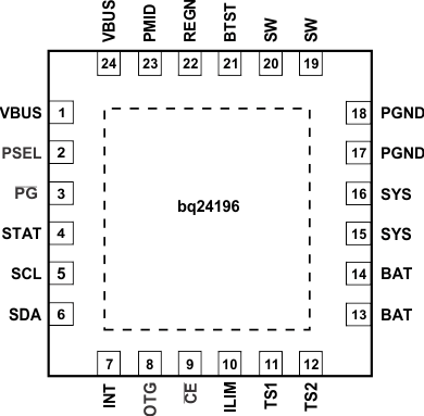
Pin Functions
| PIN | TYPE | DESCRIPTION | |
|---|---|---|---|
| NAME | NUMBER | ||
| VBUS | 1,24 | P | Charger Input Voltage. The internal n-channel reverse block MOSFET (RBFET) is connected between VBUS and PMID with VBUS on source. Place a 1-µF ceramic capacitor from VBUS to PGND and place it as close as possible to IC. (Refer to Application Information Section for details) |
| PSEL | 2 | I Digital |
Power source selection input. High indicates a USB host source and Low indicates an adapter source. |
| PG | 3 | O Digital |
Open drain active low power good indicator. Connect to the pull up rail via 10-kΩ resistor. LOW indicates a good input source if the input voltage is between UVLO and ACOV, above SLEEP mode threshold, and current limit is above 30 mA. |
| STAT | 4 | O Digital |
Open drain charge status output to indicate various charger operation. Connect to the pull up rail via 10-kΩ. LOW indicates charge in progress. HIGH indicates charge complete or charge disabled. When any fault condition occurs, STAT pin blinks at 1 Hz. |
| SCL | 5 | I Digital |
I2C Interface clock. Connect SCL to the logic rail through a 10-kΩ resistor. |
| SDA | 6 | I/O Digital |
I2C Interface data. Connect SDA to the logic rail through a 10-kΩ resistor. |
| INT | 7 | O Digital |
Open-drain Interrupt Output. Connect the INT to a logic rail via 10-kΩ resistor. The INT pin sends active low, 256-us pulse to host to report charger device status and fault. |
| OTG | 8 | I Digital |
USB current limit selection pin during buck mode, and active high enable pin during boost mode. |
| In buck mode with USB host (PSEL=High), when OTG = High, IIN limit = 500 mA and when OTG = Low, IIN limit = 100 mA. | |||
| The boost mode is activated when the REG01[5:4] = 10 and OTG pin is High. | |||
| CE | 9 | I Digital |
Active low Charge Enable pin. Battery charging is enabled when REG01[5:4] = 01 and CE pin = Low. CE pin must be pulled high or low. |
| ILIM | 10 | I Analog |
ILIM pin sets the maximum input current limit by regulating the ILIM voltage at 1 V. A resistor is connected from ILIM pin to ground to set the maximum limit as IINMAX = (1V/RILIM) × 530. The actual input current limit is the lower one set by ILIM and by I2C REG00[2:0]. The minimum input current programmed on ILIM pin is 500 mA. |
| TS1 | 11 | I Analog |
Temperature qualification voltage input #1. Connect a negative temperature coefficient thermistor. Program temperature window with a resistor divider from REGN to TS1 to GND. Charge suspends when either TS pin is out of range. Recommend 103AT-2 thermistor. |
| TS2 | 12 | I Analog |
Temperature qualification voltage input #2. Connect a negative temperature coefficient thermistor. Program temperature window with a resistor divider from REGN to TS2 to GND. Charge suspends when either TS pin is out of range. Recommend 103AT-2 thermistor. TS1 and TS2 pin can be connected together for single thermistor application. |
| BAT | 13,14 | P | Battery connection point to the positive terminal of the battery pack. The internal BATFET is connected between BAT and SYS. Connect a 10 µF closely to the BAT pin. |
| SYS | 15,16 | P | System connection point. The internal BATFET is connected between BAT and SYS. When the battery falls below the minimum system voltage, switch-mode converter keeps SYS above the minimum system voltage. (Refer to Application Information Section for inductor and capacitor selection.) |
| PGND | 17,18 | P | Power ground connection for high-current power converter node. Internally, PGND is connected to the source of the n-channel LSFET. On PCB layout, connect directly to ground connection of input and output capacitors of the charger. A single point connection is recommended between power PGND and the analog GND near the IC PGND pin. |
| SW | 19,20 | O Analog |
Switching node connecting to output inductor. Internally SW is connected to the source of the n-channel HSFET and the drain of the n-channel LSFET. Connect the 0.047-µF bootstrap capacitor from SW to BTST. |
| BTST | 21 | P | PWM high side driver positive supply. Internally, the BTST is connected to the anode of the boost-strap diode. Connect the 0.047-µF bootstrap capacitor from SW to BTST. |
| REGN | 22 | P | PWM low side driver positive supply output. Internally, REGN is connected to the cathode of the boost-strap diode. Connect a 4.7-µF (10-V rating) ceramic capacitor from REGN to analog GND. The capacitor should be placed close to the IC. REGN also serves as bias rail of TS1 and TS2 pins. |
| PMID | 23 | O Analog |
Connected to the drain of the reverse blocking MOSFET and the drain of HSFET. Given the total input capacitance, connect a 1-µF capacitor on VBUS to PGND, and the rest all on PMID to PGND. (Refer to Application Information Section for details) |
| Thermal Pad | – | P | Exposed pad beneath the IC for heat dissipation. Always solder thermal pad to the board, and have vias on the thermal pad plane star-connecting to PGND and ground plane for high-current power converter. |