SLUSBY7 July 2014
PRODUCTION DATA.
- 1 Features
- 2 Applications
- 3 Description
- 4 Revision History
- 5 Description (Continued)
- 6 Pin Configuration and Functions
- 7 Specifications
-
8 Detailed Description
- 8.1 Overview
- 8.2 Functional Block Diagram
- 8.3 Feature Description
- 8.4
Device Functional Modes
- 8.4.1 Charge Profile
- 8.4.2 EN1/EN2 Pins
- 8.4.3 I2C Operation (Host Mode / Default Mode)
- 8.4.4 External Settings: ISET, ILIM and VIN_DPM
- 8.4.5 Transient Response
- 8.4.6 Input Voltage Based DPM
- 8.4.7 Sleep Mode
- 8.4.8 Input Over-Voltage Protection
- 8.4.9 NTC Monitor
- 8.4.10 Safety Timer
- 8.4.11 Watchdog Timer
- 8.4.12 Thermal Regulation and Thermal Shutdown
- 8.4.13 Fault Modes
- 8.4.14 Serial Interface Description
- 8.5 Register Maps
- 9 Application and Implementation
- 10Power Supply Recommendations
- 11Layout
- 12Device and Documentation Support
- 13Mechanical, Packaging, and Orderable Information
Package Options
Mechanical Data (Package|Pins)
- YFF|30
Thermal pad, mechanical data (Package|Pins)
Orderable Information
11 Layout
11.1 Layout Guidelines
- Place the BOOT, PMID, IN, BAT, and LDO capacitors as close as possible to the IC for optimal performance.
- Connect the inductor as close as possible to the SW pin, and the SYS cap as close as possible to the inductor minimizing noise in the path.
- Place a 1-μF PMID capacitor as close as possible to the PMID and PGND pins, making the high frequency current loop area as small as possible.
- The local bypass capacitor from SYS to GND must be connected between the SYS pin and PGND of the IC. This minimizes the current path loop area from the SW pin through the LC filter and back to the PGND pin.
- Place all decoupling capacitors close to their respective IC pins and as close as possible to PGND (do not place components such that routing interrupts power-stage currents). All small control signals must be routed away from the high-current paths.
- To reduce noise coupling, use a ground plane if possible, to isolate the noisy traces from spreading its noise all over the board. Put vias inside the PGND pads for the IC.
- The high-current charge paths into IN, Micro-USB, BAT, SYS, and from the SW pins must be sized appropriately for the maximum charge current to avoid voltage drops in these traces.
- For high-current applications, the balls for the power paths must be connected to as much copper in the board as possible. This allows better thermal performance because the board conducts heat away from the IC.
11.2 Board Layout
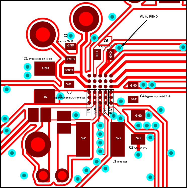 Figure 32. Recommended bq24250C PCB Layout for WCSP Package
11.3 Package Summary
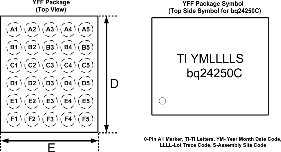
The bq24250C device is available in a 30-bump chip scale package (YFF, NanoFree™). The package dimensions are:
D – 2.427mm ±0.035mm
E – 2.027mm ±0.035mm