SLUSBY7 July 2014
PRODUCTION DATA.
- 1 Features
- 2 Applications
- 3 Description
- 4 Revision History
- 5 Description (Continued)
- 6 Pin Configuration and Functions
- 7 Specifications
-
8 Detailed Description
- 8.1 Overview
- 8.2 Functional Block Diagram
- 8.3 Feature Description
- 8.4
Device Functional Modes
- 8.4.1 Charge Profile
- 8.4.2 EN1/EN2 Pins
- 8.4.3 I2C Operation (Host Mode / Default Mode)
- 8.4.4 External Settings: ISET, ILIM and VIN_DPM
- 8.4.5 Transient Response
- 8.4.6 Input Voltage Based DPM
- 8.4.7 Sleep Mode
- 8.4.8 Input Over-Voltage Protection
- 8.4.9 NTC Monitor
- 8.4.10 Safety Timer
- 8.4.11 Watchdog Timer
- 8.4.12 Thermal Regulation and Thermal Shutdown
- 8.4.13 Fault Modes
- 8.4.14 Serial Interface Description
- 8.5 Register Maps
- 9 Application and Implementation
- 10Power Supply Recommendations
- 11Layout
- 12Device and Documentation Support
- 13Mechanical, Packaging, and Orderable Information
Package Options
Mechanical Data (Package|Pins)
- YFF|30
Thermal pad, mechanical data (Package|Pins)
Orderable Information
6 Pin Configuration and Functions
YFF Package
(30-Ball 2.4 mm × 2 mm DSBGA)
Top View
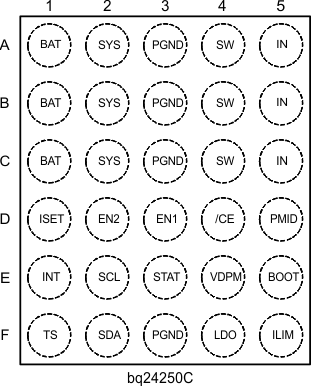
Pin Descriptions
| PIN NAME |
bq24250C | bq24250C | I/O | DESCRIPTION |
|---|---|---|---|---|
| YFF | RGE | |||
| AGND | – | 4 | Analog Ground for QFN only. Connect to the thermal pad and the ground plane of the circuit. | |
| BAT | A1, B1, C1 | 11–12 | I/O | Battery Connection. Connect to the positive pin of the battery. Additionally, bypass BAT with a >1μF capacitor. |
| BOOT | E5 | 21 | I | High Side MOSFET Gate Driver Supply. Connect a 0.033μF ceramic capacitor (voltage rating > 15V) from BOOT to SW to supply the gate drive for the high side MOSFETs. |
| CE | D4 | 1 | I | Charge Enable Active-Low Input. Connect CE to a high logic level to place the battery charger in standby mode. |
| CHG | – | – | O | Charge Status Open Drain Output. CHG is pulled low when a charge cycle starts and remains low while charging. CHG is high impedance when the charging terminates and when no supply exists. CHG does not indicate recharge cycles. |
| EN1 | D3 | 2 | I | Input Current Limit Configuration Inputs. Use EN1, and EN2 to control the maximum input current and enable USB compliance. See Table 1 for programming details. |
| EN2 | D2 | 3 | I | |
| ILIM | F5 | 22 | I | Input Current Limit Programming Input. Connect a resistor from ILIM to GND to program the input current limit for IN. The current limit is programmable from 0.5A to 2A. ILIM has no effect on the USB input. If an external resistor is not desired, short to GND for a 2A default setting. |
| IN | A5,B5,C5 | 19 | I | Input power supply. IN is connected to the external DC supply (AC adapter or USB port). Bypass IN to PGND with >2μF ceramic capacitor |
| INT | E1 | 8 | O | Status Output. INT is an open-drain output that signals charging status and fault interrupts. INT pulls low during charging. INT is high impedance when charging is complete or the charger is disabled. When a fault occurs, a 256μs pulse is sent out as an interrupt for the host. INT will indicate recharge cycles. Connect INT to a logic rail through a 10kΩ resistor to communicate with the host processor. |
| ISET | D1 | 10 | I | Charge Current Programming Input. Connect a resistor from ISET to GND to program the fast charge current. The charge current is programmable from 300mA to 2A. |
| LDO | F4 | 24 | O | LDO output. LDO is regulated to 4.9V and drives up to 50mA. Bypass LDO with a 1μF ceramic Capacitor. LDO is enabled when VUVLO < VIN <18V. |
| PGND | A3, B3, C3, F3 | 15–16 | Ground pin. Connect to the ground plane of the circuit. | |
| PMID | D5 | 20 | I | Connection between blocking FET and high-side FET. |
| SCL | E2 | 6 | I | I2C Interface Clock. Connect SCL to the logic rail through a 10kΩ resistor. |
| SDA | F2 | 5 | I/O | I2C Interface Data. Connect SDA to the logic rail through a 10kΩ resistor. |
| STAT | E3 | 7 | O | Status Output. STAT is an open-drain output that signals charging status and fault interrupts. STAT pulls low during charging. STAT is high impedance when charging is complete or the charger is disabled. When a fault occurs, a 256μs pulse is sent out as an interrupt for the host. STAT is enabled/disabled using the EN_STAT bit in the control register. STAT will indicate recharge cycles. Connect STAT to a logic rail using an LED for visual indication or through a 10kΩ resistor to communicate with the host processor. |
| SW | A4, B4, C4 | 17–18 | O | Inductor Connection. Connect to the switching side of the external inductor. |
| SYS | A2, B2, C2 | 13–14 | I | System Voltage Sense and SMPS output filter connection. Connect SYS to the system output at the output bulk capacitors. Bypass SYS locally with >20μF. |
| TS | F1 | 9 | I | Battery Pack NTC Monitor. Connect TS to the center tap of a resistor divider from LDO to GND. The NTC is connected from TS to GND. See the NTC Monitor section for more details on operation and selecting the resistor values. |
| VDPM | E4 | 23 | I | Input DPM Programming Input. Connect a resistor divider between IN and GND with VDPM connected to the center tap to program the Input Voltage based Dynamic Power Management threshold (VIN_DPM). The input current is reduced to maintain the supply voltage at VIN_DPM. The reference for the regulator is 1.2V. Short pin to GND if external resistors are not desired—this sets a default of 4.68V for the input DPM threshold (EN1=1,EN2=0). |