SLUSBZ9C August 2015 – September 2016 BQ25120 , BQ25121
PRODUCTION DATA.
- 1 Features
- 2 Applications
- 3 Description
- 4 Revision History
- 5 Description (continued)
- 6 Device Comparison Table
- 7 Pin Configuration and Functions
- 8 Specifications
-
9 Detailed Description
- 9.1 Overview
- 9.2 Functional Block Diagram
- 9.3
Feature Description
- 9.3.1 Ship Mode
- 9.3.2 High Impedance Mode
- 9.3.3 Active Battery Only Connected
- 9.3.4 Voltage Based Battery Monitor
- 9.3.5 Sleep Mode
- 9.3.6 Input Voltage Based Dynamic Power Management (VIN(DPM))
- 9.3.7 Input Overvoltage Protection and Undervoltage Status Indication
- 9.3.8 Battery Charging Process and Charge Profile
- 9.3.9 Dynamic Power Path Management Mode
- 9.3.10 Battery Supplement Mode
- 9.3.11 Default Mode
- 9.3.12 Termination and Pre-Charge Current Programming by External Components (IPRETERM)
- 9.3.13 Input Current Limit Programming by External Components (ILIM)
- 9.3.14 Charge Current Programming by External Components (ISET)
- 9.3.15 Safety Timer and Watchdog Timer
- 9.3.16 External NTC Monitoring (TS)
- 9.3.17 Thermal Protection
- 9.3.18 Typical Application Power Dissipation
- 9.3.19 Status Indicators (PG and INT)
- 9.3.20 Chip Disable (CD)
- 9.3.21 Buck (PWM) Output
- 9.3.22 Load Switch / LDO Output and Control
- 9.3.23 Manual Reset Timer and Reset Output (MR and RESET)
- 9.4 Device Functional Modes
- 9.5 Programming
- 9.6
Register Maps
- 9.6.1 Status and Ship Mode Control Register
- 9.6.2 Faults and Faults Mask Register
- 9.6.3 TS Control and Faults Masks Register
- 9.6.4 Fast Charge Control Register
- 9.6.5 Termination/Pre-Charge and I2C Address Register
- 9.6.6 Battery Voltage Control Register
- 9.6.7 SYS VOUT Control Register
- 9.6.8 Load Switch and LDO Control Register
- 9.6.9 Push-button Control Register
- 9.6.10 ILIM and Battery UVLO Control Register
- 9.6.11 Voltage Based Battery Monitor Register
- 9.6.12 VIN_DPM and Timers Register
- 10Application and Implementation
- 11Power Supply Recommendations
- 12Layout
- 13Device and Documentation Support
- 14Mechanical, Packaging, and Orderable Information
Package Options
Mechanical Data (Package|Pins)
- YFP|25
Thermal pad, mechanical data (Package|Pins)
Orderable Information
10 Application and Implementation
NOTE
Information in the following applications sections is not part of the TI component specification, and TI does not warrant its accuracy or completeness. TI's customers are responsible for determining suitability of components for their purposes. Customers should validate and test their design implementation to confirm system functionality.
10.1 Application Information
A typical design is shown in Figure 35. This design uses the BQ25120 with external resistors for ILIM, IPRETERM, and ISET. These are not needed if these values are set with a host controller through I2C commands. This design also shows the TS resistors, which is also optional.
When powering up in default mode the battery voltage is the default for the part (4.2 V), the SYS output is the default (1.8 V). External resistors set the charge current to 40 mA, the termination current to 10% (4 mA), and the input current limit to 100 mA. If the I2C interface is used the part goes to the internal default settings until changed by the host.
10.2 Typical Application
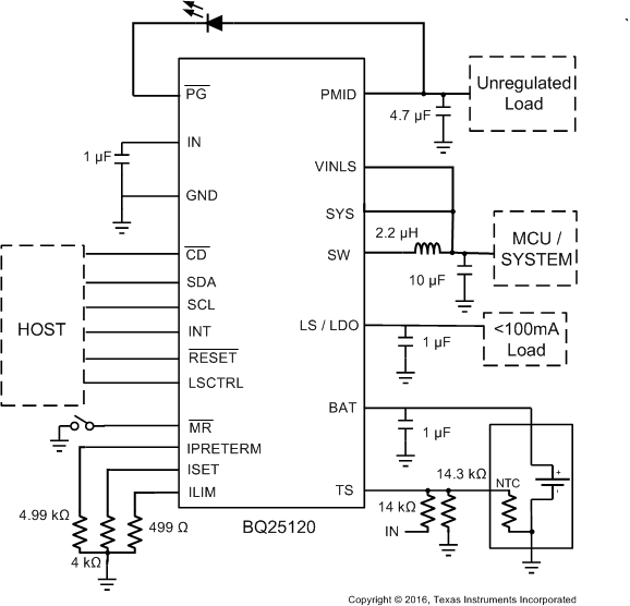 Figure 35. Typical Application Circuit
10.2.1 Design Requirements
This application is for a low power system that has varying loads from less than 10 mA up to 300 mA. It must work with a valid adaptor or USB power input. Below are some of the key components that are needed in normal operation. For this example, the fast charge current is 50 mA, input current limit is 400 mA and the pre-charge and termination current is 10% of the fast charge current.
- Supply voltage = 3.4 V to 20 V
- Fast charge current is default to 10 mA with ISET pin shorted to ground. To program the fast charge current, connect an external resistor from ISET to ground.
- Input current limit is default to 100 mA with ILIM pin shorted to ground. To program the input current limit, connect an external resistor from ILIM to ground.
- Termination current threshold is default to 2 mA with IPRETERM pin shorted to ground. To program the input current limit, connect an external resistor from IPRETERM to ground.
- A 2.2-µH inductor is needed between SW pin and SYS pin for PWM output.
- TS- Battery temperature sense needs a NTC connected on TS pin.
10.2.2 Detailed Design Procedure
See Figure 35 for an example of the application diagram.
10.2.2.1 Default Settings
- • Connect ISET, ILIM and IPRETERM pins to ground to program fast charge current to 10mA, input current limit to 100mA and pre-charge/termination current to 2 mA.
- BAT_UVLO = 3 V.
- VSYS = 1.8 V
- LS/LDO is LS
- VBREG = 4.2 V
- VIN_DPM is enabled and VIN_DPM Threshold = 4.6 V.
- Safety Timer = 3 hr
- If the function is not needed, connect TS to the center tab of the resistor divider between VIN and the ground. (pull up resistor = 14 kΩ, pull down resistor = 14.3 kΩ)
10.2.2.2 Choose the Correct Inductance and Capacitance
Refer to the Buck (PWM) Output section for the detailed procedure to determine the optimal inductance and capacitance for the buck output.
10.2.2.3 Calculations
10.2.2.3.1 Program the Fast Charge Current (ISET)
KISET = 200 AΩ from the Specifications table
Select the closest standard value, which in this case is 4.99 kΩ. Connect this resistor between ISET pin and GND.
10.2.2.3.2 Program the Input Current Limit (ILIM)
KILIM = 200 AΩ from the Specifications table
Select the closest standard value, which in this case is 499 Ω. Connect this resistor between ILIM pin and GND.
10.2.2.3.3 Program the Pre-charge/termination Threshold (IPRETERM)
According to Table 3, the RIPRETERM is 4990 Ω for 10% termination threshold. Therefore, connect a 4.99 kΩ resistor between IPRETERM pin and GND.
10.2.2.3.4 TS Resistors (TS)
The voltage at TS is monitored to determine that the battery is at a safe temperature during charging. This device uses JEITA temperature profile which has four temperature thresholds. Refer to Specifications for the detailed thresholds number.
The TS circuit is shown in Figure 16. The resistor values can be calculated using Equation 1 and Equation 2.
10.2.3 Application Performance Curves
10.2.3.1 Charger Curves
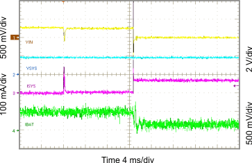
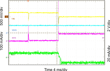
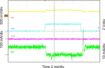
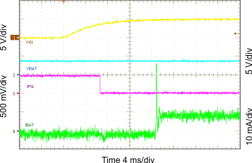
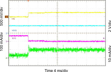
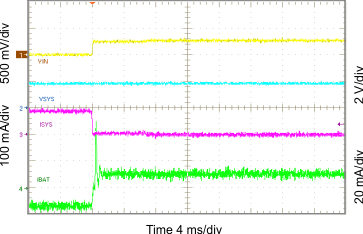
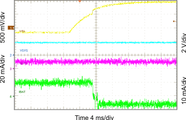
10.2.3.2 SYS Output Curves
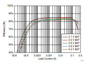
| TA = 25°C | VSYS = 1.2 V |
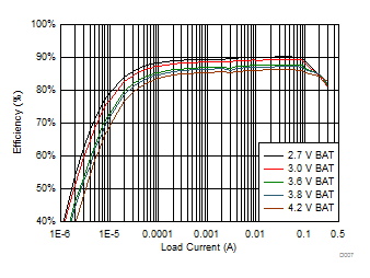
| TA = 25°C | VSYS = 1.8 V |
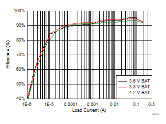
| TA = 25°C | VSYS = 3.3 V |
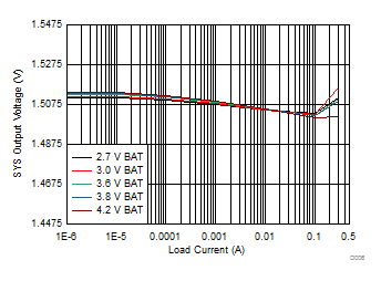
| TA = 25°C | VSYS = 1.5 V |
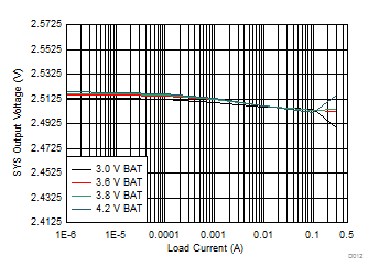
| TA = 25°C | VSYS = 2.5 V |
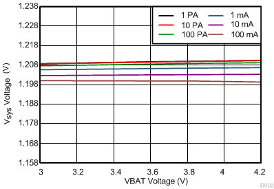
| TA = 25°C | VSYS = 1.2 V |
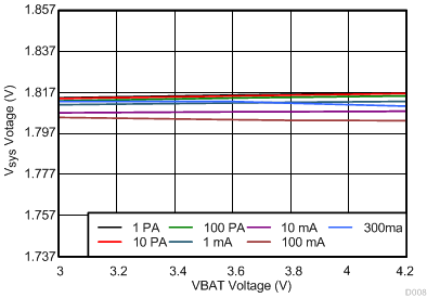
| TA = 25°C | VSYS = 1.8 V |
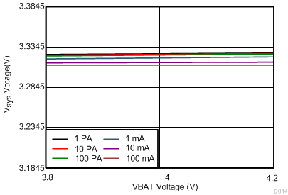
| TA = 25°C | VSYS = 3.3 V |
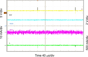
| ILOAD = 10 µA |
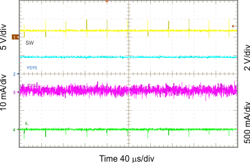
| ILOAD = 1 mA |
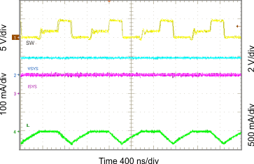
| ILOAD = 100 mA |
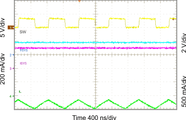
| ILOAD = 300 mA |
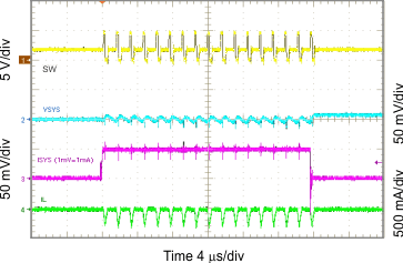
| VSYS = 1.8 V |
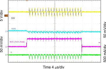
| VSYS = 2.5 V |
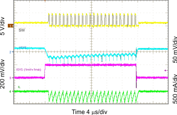
| VSYS = 1.2 V |
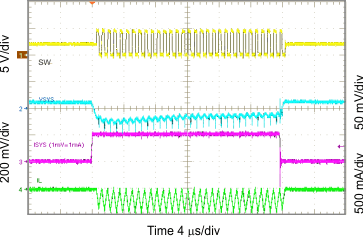
| VSYS = 2.1 V |
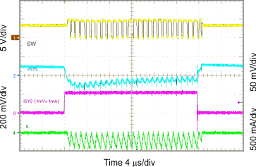
| VSYS = 3.3 V |
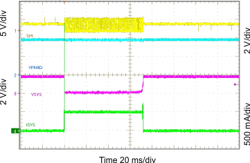
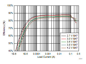
| TA = 25°C | VSYS = 1.5 V |
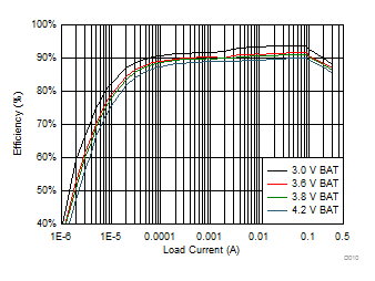
| TA = 25°C | VSYS = 2.5 V |
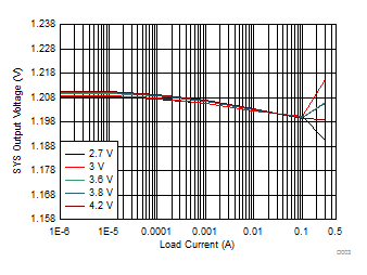
| TA = 25°C | VSYS = 1.2 V |
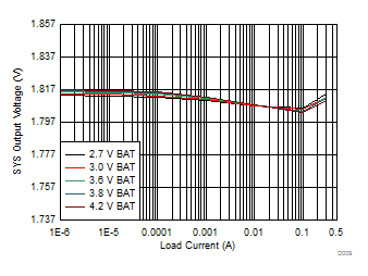
| TA = 25°C | VSYS = 1.8 V |
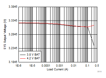
| TA = 25°C | VSYS = 3.3 V |
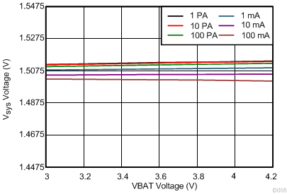
| TA = 25°C | VSYS = 1.5 V |
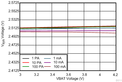
| TA = 25°C | VSYS = 2.1 V |
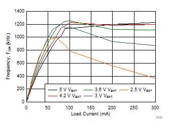
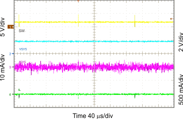
| ILOAD = 100 mA |
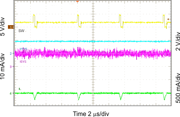
| ILOAD = 10 mA |
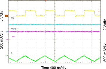
| ILOAD = 200 mA |
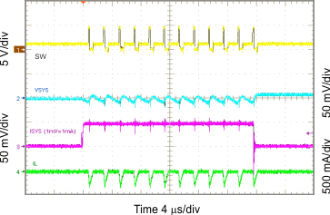
| VSYS = 1.2 V |
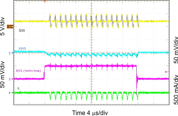
| VSYS = 2.1 V |
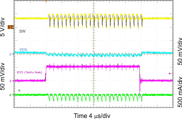
| VSYS = 3.3 V |
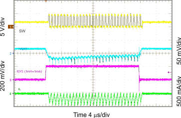
| VSYS = 1.8 V |
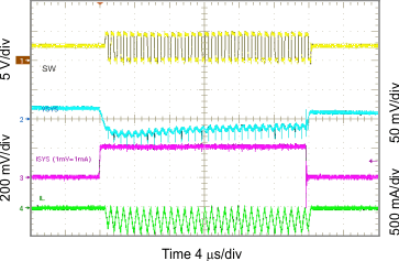
| VSYS = 2.5 V |
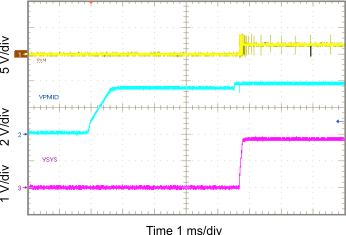
10.2.3.3 Load Switch and LDO Curves
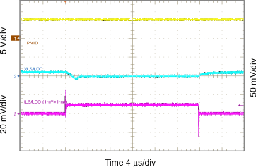
| VSLSDO = 0.8 V |
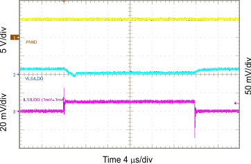
| VSLSDO = 1.8 V |
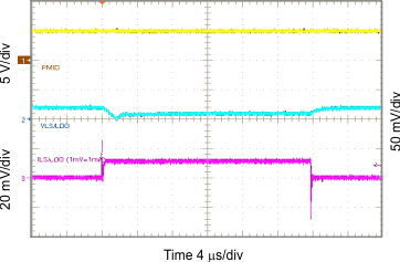
| VSLSDO = 3.3 V |
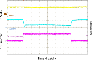
| VSLSDO = 1.2 V |
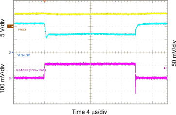
| VSLSDO = 2.5 V |
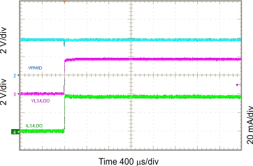
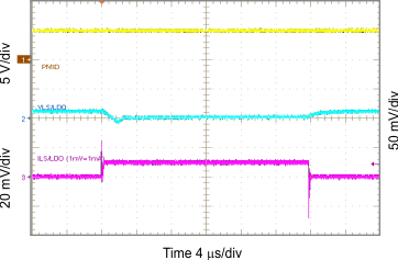
| VSLSDO = 1.2 V |
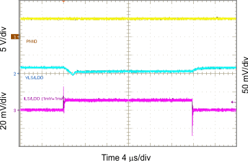
| VSLSDO = 2.5 V |
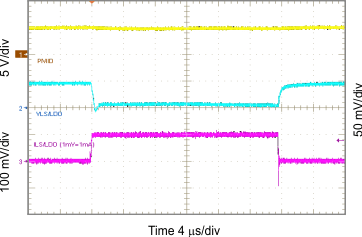
| VSLSDO = 0.8 V |
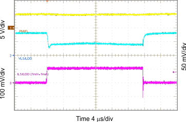
| VSLSDO = 1.8 V |
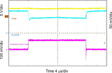
| VSLSDO = 3.3 V |
10.2.3.4 LS/LDO Output Curves
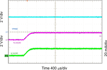
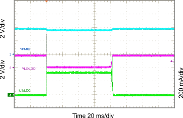
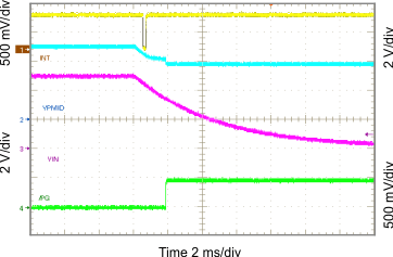
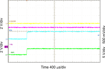
10.2.3.5 Timing Waveforms Curves
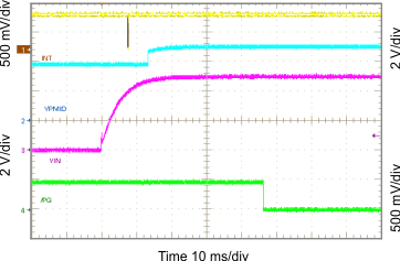
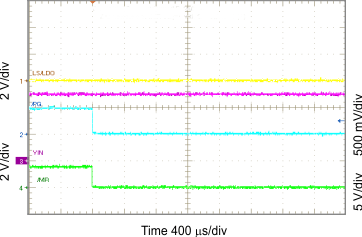
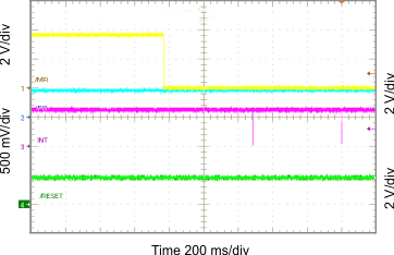
| Wake1 = 500 ms | Wake2 = 1 s |
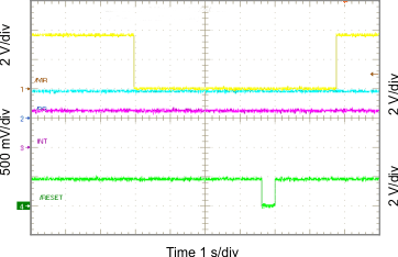
| RESET = 4 s |
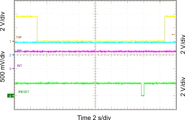
| RESET = 14 s |
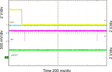
| Wake1 = 50 ms | Wake2 = 1.5 s |
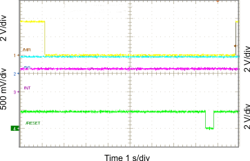
| RESET = 8 s |
