SLUSCI1B August 2016 – November 2016
PRODUCTION DATA.
- 1 Features
- 2 Applications
- 3 Description
- 4 Revision History
- 5 Pin Configuration and Functions
-
6 Specifications
- 6.1 Absolute Maximum Ratings
- 6.2 ESD Ratings
- 6.3 Recommended Operating Conditions
- 6.4 Thermal Information
- 6.5 Electrical Characteristics: Supply Current
- 6.6 Electrical Characteristics: Digital Input and Output DC Characteristics
- 6.7 Electrical Characteristics: Power-On Reset
- 6.8 Electrical Characteristics: LDO Regulator
- 6.9 Electrical Characteristics: Internal Temperature Sensor
- 6.10 Electrical Characteristics: Low-Frequency Clock Oscillator
- 6.11 Electrical Characteristics: High-Frequency Clock Oscillator
- 6.12 Electrical Characteristics: Integrating ADC (Coulomb Counter)
- 6.13 Electrical Characteristics: ADC (Temperature and Voltage Measurements)
- 6.14 Electrical Characteristics: Data Flash Memory
- 6.15 Timing Requirements: I2C-Compatible Interface Timing Characteristics
- 6.16 Typical Characteristics
- 7 Detailed Description
- 8 Application and Implementation
- 9 Power Supply Recommendations
- 10Layout
- 11Device and Documentation Support
- 12Mechanical, Packaging, and Orderable Information
Package Options
Mechanical Data (Package|Pins)
- PW|14
Thermal pad, mechanical data (Package|Pins)
- PW|14
Orderable Information
9 Power Supply Recommendations
Power supply requirements for the bq34110 device are simplified due to the presence of the internal LDO-voltage regulation. The REGIN pin accepts any voltage level between 2.7 V and 4.5 V, which is optimum for a single-cell Li-Ion application. For higher battery voltage applications, a simple preregulator can be provided to power the bq34110 device. Decoupling the REGIN pin should be done with a 0.1-μF 10% ceramic X5R capacitor placed close to the device. While the preregulator circuit is not critical, special attention should be paid to its quiescent current and power dissipation. The input voltage should handle the maximum battery stack voltage. The output voltage can be centered within the 2.7-V to 4.5-V range as recommended for the REGIN pin.
For high stack count applications, a commercially available LDO is often the best quality solution, but comes with a cost tradeoff. To lower the BOM cost, the following approaches are recommended.
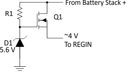
In Figure 17, Q1 is used to drop the battery stack voltage to roughly 4 V to power the bq34110 device's REGIN pin. To avoid unwanted quiescent current consumption, R1 should be set as high as is practical. It is recommended to use a low-current Zener diode.
 Figure 17. Q1 Dropping Battery Stack Voltage to 4 V
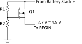
Alternatively, if the range of a high-voltage battery stack can be well-defined, a simple source follower based on a resistive divider can be used to lower the BOM cost and the quiescent current. For example:
 Figure 18. Source Follower on a Resistive Divider