SLUSBB8A December 2012 – June 2016
PRODUCTION DATA.
- 1 Features
- 2 Applications
- 3 Description
- 4 Revision History
- 5 Device Comparison Tables
- 6 Pin Configuration and Functions
- 7 Specifications
-
8 Detailed Description
- 8.1 Overview
- 8.2 Functional Block Diagram
- 8.3
Feature Description
- 8.3.1 Qi Wireless Power System and bq51010B Power Transfer Flow Diagrams
- 8.3.2 Dynamic Rectifier Control
- 8.3.3 Dynamic Efficiency Scaling
- 8.3.4 RILIM Calculations
- 8.3.5 Input Overvoltage
- 8.3.6 Adapter Enable Functionality and EN1 or EN2 Control
- 8.3.7 End Power Transfer Packet (WPC Header 0x02)
- 8.3.8 Status Outputs
- 8.3.9 WPC Communication Scheme
- 8.3.10 Communication Modulator
- 8.3.11 Adaptive Communication Limit
- 8.3.12 Synchronous Rectification
- 8.3.13 Temperature Sense Resistor Network (TS)
- 8.3.14 3-State Driver Recommendations For the TS-CTRL Pin
- 8.3.15 Thermal Protection
- 8.3.16 WPC 1.1 Compliance - Foreign Object Detection
- 8.4 Device Functional Modes
-
9 Application and Implementation
- 9.1 Application Information
- 9.2 Typical Applications
- 10Power Supply Recommendations
- 11Layout
- 12Device and Documentation Support
- 13Mechanical, Packaging, and Orderable Information
Package Options
Mechanical Data (Package|Pins)
- YFP|28
Thermal pad, mechanical data (Package|Pins)
Orderable Information
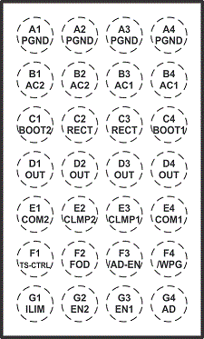
6 Pin Configuration and Functions
YFP Package
28-Pin DSBGA
Top View

Pin Functions
| PIN | I/O | DESCRIPTION | |
|---|---|---|---|
| NAME | NO. | ||
| AC1 | B3, B4 | I | AC input from receiver coil antenna. |
| AC2 | B1, B2 | I | |
| AD | G4 | I | Connect this pin to the wired adapter input. When a voltage is applied to this pin wireless charging is disabled and AD_EN is driven low. Connect to GND through a 1-µF capacitor. If unused, capacitor is not required and must be grounded directly. |
| AD-EN | F3 | O | Push-pull driver for external PFET connecting AD and OUT. This node is pulled to the higher of OUT and AD when turning off the external FET. This voltage tracks approximately 4 V below AD when voltage is present at AD and provides a regulated VSG bias for the external FET. Float this pin if unused. |
| BOOT1 | C4 | O | Bootstrap capacitors for driving the high-side FETs of the synchronous rectifier. Connect a 10-nF ceramic capacitor from BOOT1 to AC1 and from BOOT2 to AC2. |
| BOOT2 | C1 | O | |
| CLMP1 | E3 | O | Open drain FETs are used for a non-power dissipative overvoltage AC clamp protection. When the RECT voltage goes above 15 V, both switches is turned on and the capacitors acts as a low impedance to protect the IC from damage. If used, Clamp1 is required to be connected to AC1, and Clamp2 is required to be connected to AC2 through 0.47-µF capacitors. |
| CLMP2 | E2 | O | |
| COM1 | E4 | O | Open-drain output used to communicate with primary by varying reflected impedance. Connect through a capacitor to either AC1 or AC2 for capacitive load modulation (COM2 must be connected to the alternate AC1 or AC2 pin). For resistive modulation connect COM1 and COM2 to RECT through a single resistor; connect through separate capacitors for capacitive load modulation. |
| COM2 | E1 | O | |
| EN1 | G3 | I | Inputs that allow user to enable or disable wireless and wired charging <EN1 EN2>: <00> wireless charging is enabled unless AD voltage > 3.6 V <01> Dynamic communication current limit disabled <10> AD-EN pulled low, wireless charging disabled <11> wired and wireless charging disabled. |
| EN2 | G2 | I | |
| FOD | F2 | I | Input for the received power measurement. Connect to GND with a 140-Ω resistor. See the FOD section for more detail. |
| ILIM | G1 | I/O | Programming pin for the over current limit. Connect external resistor to VSS. Size RILIM with the following equation: RILIM = 314 / IMAX where IMAX is the expected maximum output current of the wireless power supply. The hardware current limit (IILIM) is 20% greater than IMAX or 1.2 x 1MAX. If the supply is meant to operate in current limit use: RILIM = 314 / IILIM, RILIM = R1 + RFOD |
| OUT | D1, D2, D3, D4 |
O | Output pin, delivers power to the load. |
| PGND | A1, A2, A3, A4 |
— | Power ground |
| RECT | C2, C3 | O | Filter capacitor for the internal synchronous rectifier. Connect a ceramic capacitor to PGND. Depending on the power levels, the value may be 4.7 μF to 22 μF. |
| TS/CTRL | F1 | I | Must be connected to ground through a resistor. If an NTC function is not desired connect to GND with a 10-kΩ resistor. As a CTRL pin pull to ground to send end power transfer (EPT) fault to the transmitter or pull-up to an internal rail (that is, 1.8 V) to send EPT termination to the transmitter. Note that a 3-state driver must be used to interface this pin (see the 3-State Driver Recommendations For the TS-CTRL Pin section for further description) |
| WPG | F4 | O | Open-drain output – Active when the output of the wireless power supply is enabled. |