SLUSC16B November   2015  – March 2019

PRODUCTION DATA.  

  1. Features
  2. Applications
  3. Description
    1.     Device Images
      1.      Simplified Schematic
  4. Revision History
  5. Pin Configuration and Functions
    1.     Pin Functions
  6. Specifications
    1. 6.1 Absolute Maximum Ratings
    2. 6.2 ESD Ratings
    3. 6.3 Recommended Operating Conditions
    4. 6.4 Thermal Information
    5. 6.5 Electrical Characteristics
    6. 6.6 Timing Requirements
    7. 6.7 Typical Characteristics
  7. Detailed Description
    1. 7.1 Overview
    2. 7.2 Functional Block Diagram
    3. 7.3 Feature Description
      1. 7.3.1 Charge Pump Control
      2. 7.3.2 Pin Enable Controls
        1. 7.3.2.1 External Control of CHG and DSG Output Drivers
        2. 7.3.2.2 External Control of PCHG Output Driver
        3. 7.3.2.3 Pack Monitor Enable
    4. 7.4 Device Functional Modes
  8. Application and Implementation
    1. 8.1 Application Information
      1. 8.1.1 Recommended System Implementation
        1. 8.1.1.1 bq76200 Slave Device
        2. 8.1.1.2 Flexible Control via AFE or via MCU
        3. 8.1.1.3 Scalable VDDCP Capacitor to Support Multiple FETs in Parallel
        4. 8.1.1.4 Precharge and Predischarge Support
        5. 8.1.1.5 Optional External Gate Resistor
        6. 8.1.1.6 Separate Charge and Discharge paths
    2. 8.2 Typical Applications
      1. 8.2.1 Design Requirements
      2. 8.2.2 Detailed Design Procedure
      3. 8.2.3 Application Curves
  9. Power Supply Recommendations
  10. 10Layout
    1. 10.1 Layout Guidelines
    2. 10.2 Layout Example
  11. 11Device and Documentation Support
    1. 11.1 Documentation Support
      1. 11.1.1 Related Documentation
    2. 11.2 Community Resources
    3. 11.3 Trademarks
    4. 11.4 Electrostatic Discharge Caution
    5. 11.5 Glossary
  12. 12Mechanical, Packaging, and Orderable Information

Package Options

Mechanical Data (Package|Pins)
Thermal pad, mechanical data (Package|Pins)
Orderable Information

Separate Charge and Discharge paths

In some systems, the charging current might be significantly lower than the discharge current. In such systems, the system designer may prefer to implement a separate charge and discharge paths in which the number of FET in parallel for charge and discharge can be different to reduce to BOM cost.
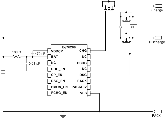
bq76200 Apps3.gifFigure 11. Separate Charge and Discharge Paths (Partial Schematic Shown)