SLUSC16B November 2015 – March 2019
PRODUCTION DATA.
- 1 Features
- 2 Applications
- 3 Description
- 4 Revision History
- 5 Pin Configuration and Functions
- 6 Specifications
- 7 Detailed Description
- 8 Application and Implementation
- 9 Power Supply Recommendations
- 10Layout
- 11Device and Documentation Support
- 12Mechanical, Packaging, and Orderable Information
Package Options
Mechanical Data (Package|Pins)
- PW|16
Thermal pad, mechanical data (Package|Pins)
Orderable Information
6.6 Timing Requirements
| Parameter | Description | TEST CONDITION | MIN | TYP | MAX | UNIT |
|---|---|---|---|---|---|---|
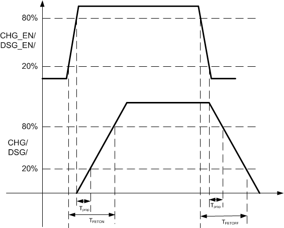
| tCHGFETON | CHG on rise time + propagation delay | CL = 10 nF, (20% of CHG_EN from Lo to Hi) to (80% of V(CHGFETON)), CP_EN = Hi, (CP is already on) | 27 | 45 | µs | |
| tCHGFETOFF | CHG off fall time + propagation delay | CL= 10 nF, (80% of CHG_EN from Hi to Lo) to (20% of V(CHGFETON)) , CHG_EN = Hi to Lo | 7 | 20 | µs | |
| tPROP_CHG | CHG EN to CHG output | CL= 10 nF, CP_EN = Hi, (CP is already on), see timing diagram | 0.5 | µs | ||
| tDSGFETON | DSG on rise time + propagation delay | CL = 10 nF, (20% of DSG_EN from Lo to Hi) to (80% of V(DSGFETON)), CP_EN = Hi, (CP is already on) | 24 | 50 | µs | |
| tDSGFETOFF | DSG off fall time + propagation delay | CL = 10 nF, (80% of DSG_EN from Hi to Lo) to (20% of V(DSGFETON)) | 7 | 20 | µs | |
| tPROP_DSG | DSG EN to DSG output propagation delay | CL= 10 nF, CP_EN = Hi, (CP already on), see timing Diagram | 0.5 | µs | ||
| tPCHGOFF | PCHG turn off time + propagation delay | CL = 1 nF, (20% of PCHG_EN from Hi to Lo) to (80% of VPCHGFETON) | 30 | 60 | µs | |
| tPCHGON | PCHG turn on time + propagation delay | CL = 1 nF, (80% of PCHG_EN from Lo to Hi) to (20% of V(PCHGFETON)) | 34 | 55 | µs | |
| tPROP_PCHG | PCH_EN to PCHG propagation delay | CL = 1 nF | 0.5 | µs | ||
| tPROP_PMON | PMON_EN and PACKDIV = PACK propagation delay | 0.5 | µs |
 Figure 1. Timing Characteristics - ( CP assumed to be already On)