SWRS111F June 2011 – October 2014 CC1121
PRODUCTION DATA.
- 1Device Overview
- 2Revision History
- 3Terminal Configuration and Functions
-
4Specifications
- 4.1 Absolute Maximum Ratings
- 4.2 Handling Ratings
- 4.3 Recommended Operating Conditions (General Characteristics)
- 4.4 Thermal Resistance Characteristics for RHB Package
- 4.5 RF Characteristics
- 4.6 Regulatory Standards
- 4.7 Current Consumption, Static Modes
- 4.8 Current Consumption, Transmit Modes
- 4.9 Current Consumption, Receive Modes
- 4.10
Receive Parameters
- 4.10.1 General Receive Parameters (High-Performance Mode)
- 4.10.2 RX Performance in 950-MHz Band (High-Performance Mode)
- 4.10.3 RX Performance in 868-, 915-, and 920-MHz Bands (High-Performance Mode)
- 4.10.4 RX Performance in 434-MHz Band (High-Performance Mode)
- 4.10.5 RX Performance in 169-MHz Band (High-Performance Mode)
- 4.10.6 RX Performance in Low-Power Mode
- 4.11 Transmit Parameters
- 4.12 PLL Parameters
- 4.13 Wake-up and Timing
- 4.14 32-MHz Crystal Oscillator
- 4.15 32-MHz Clock Input (TCXO) data to TCXO table
- 4.16 32-kHz Clock Input
- 4.17 32-kHz RC Oscillator
- 4.18 I/O and Reset
- 4.19 Temperature Sensor
- 4.20 Typical Characteristics
- 5Detailed Description
- 6Typical Application Circuit
- 7Device and Documentation Support
- 8Mechanical Packaging and Orderable Information
Package Options
Mechanical Data (Package|Pins)
- RHB|32
Thermal pad, mechanical data (Package|Pins)
- RHB|32
Orderable Information
6 Typical Application Circuit
NOTE
This section is intended only as an introduction.
Very few external components are required for the operation of the CC1121 device. Figure 6-1 shows a typical application circuit. The board layout will greatly influence the RF performance of the CC1121 device. Figure 6-1 does not show decoupling capacitors for power pins.
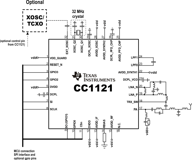 Figure 6-1 Typical Application Circuit
For more information, see the reference designs available for the CC1121 device in Section 7.2, Documentation Support.