SWAS031D June 2013 – February 2015 CC3100
PRODUCTION DATA.
- 1Device Overview
- 2Revision History
- 3Terminal Configuration and Functions
-
4Specifications
- 4.1 Absolute Maximum Ratings
- 4.2 Handling Ratings
- 4.3 Power-On Hours
- 4.4 Recommended Operating Conditions
- 4.5 Brown-Out and Black-Out
- 4.6 Electrical Characteristics (3.3 V, 25°C)
- 4.7 WLAN Receiver Characteristics
- 4.8 WLAN Transmitter Characteristics
- 4.9 Current Consumption
- 4.10 Thermal Characteristics for RGC Package
- 4.11 Timing and Switching Characteristics
- 4.12 External Interfaces
- 4.13 Host UART
- 5Detailed Description
- 6Applications and Implementation
- 7Device and Documentation Support
- 8Mechanical Packaging and Orderable Information
Package Options
Mechanical Data (Package|Pins)
- RGC|64
Thermal pad, mechanical data (Package|Pins)
- RGC|64
Orderable Information
3 Terminal Configuration and Functions
Figure 3-1 shows pin assignments for the 64-pin QFN package.
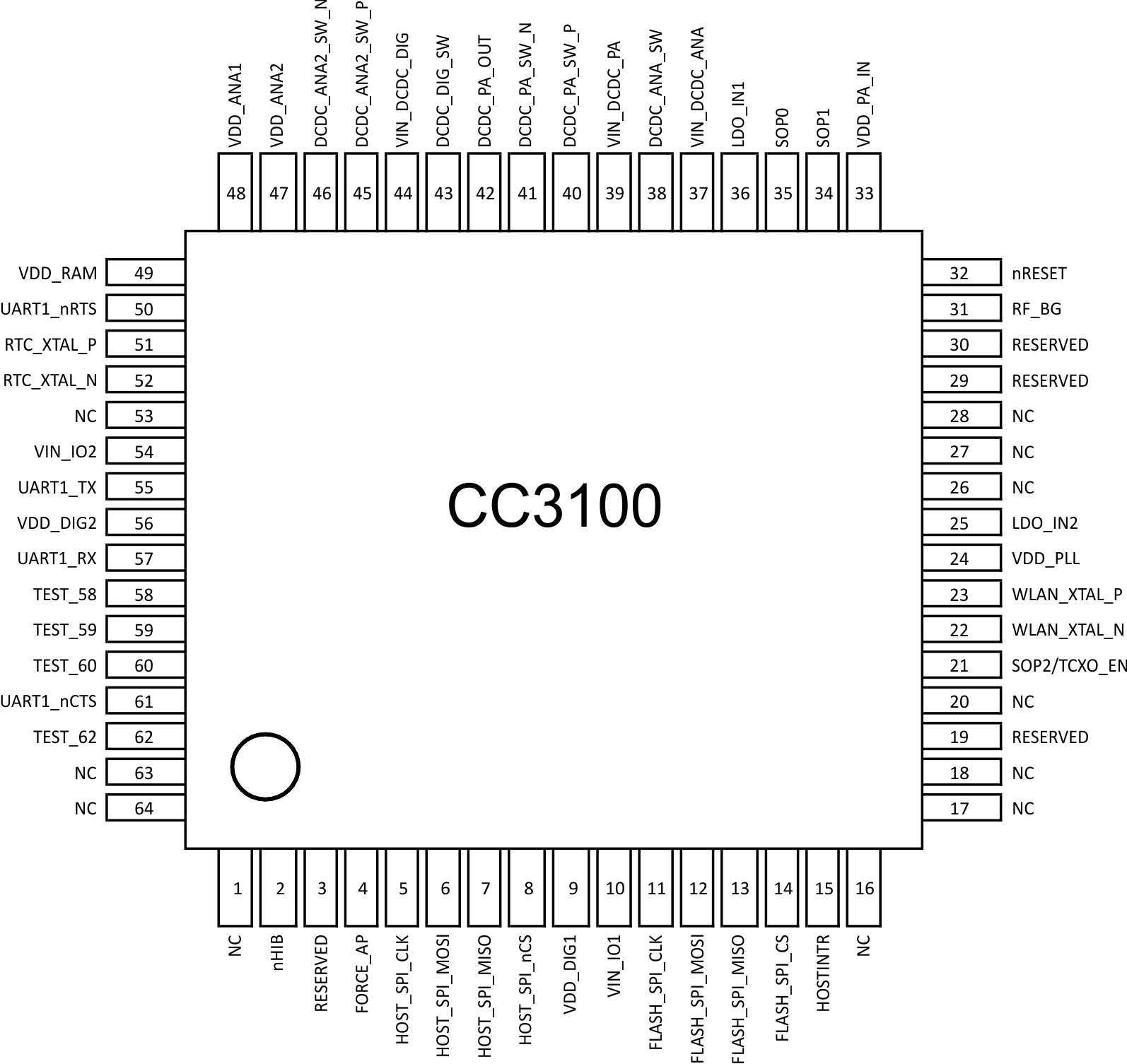
3.1 Pin Attributes
Table 3-1 describes the CC3100 pins.
NOTE
If an external device drives a positive voltage to signal pads when the CC3100 device is not powered, DC current is drawn from the other device. If the drive strength of the external device is adequate, an unintentional wakeup and boot of the CC3100 device can occur. To prevent current draw, TI recommends one of the following:
- All devices interfaced to the CC3100 device must be powered from the same power rail as the CC3100 device.
- Use level-shifters between the CC3100 device and any external devices fed from other independent rails.
- The nRESET pin of the CC3100 device must be held low until the VBAT supply to the device is driven and stable.
Table 3-1 Pin Attributes
| PIN | DEFAULT FUNCTION | STATE AT RESET AND HIBERNATE | I/O TYPE | DESCRIPTION |
|---|---|---|---|---|
| 1 | NC | Hi-Z | N/A | Unused; leave unconnected. |
| 2 | nHIB | Hi-Z | I | Hibernate signal input to the NWP (active low). This is connected to the MCU GPIO. If the GPIO from the MCU can float while the MCU enters low power, consider adding a pull-up resistor on the board to avoid floating. |
| 3 | Reserved | Hi-Z | NA | Reserved for future use |
| 4 | FORCE_AP | Hi-Z | I | For forced AP mode, pull to high on the board using 100k resistor. Otherwise, pull down to ground using 100k resistor.(1) |
| 5 | HOST_SPI_CLK | Hi-Z | I | Host interface SPI clock |
| 6 | HOST_SPI_MOSI | Hi-Z | I | Host interface SPI data input |
| 7 | HOST_SPI_MISO | Hi-Z | O | Host interface SPI data output |
| 8 | HOST_SPI_nCS | Hi-Z | I | Host interface SPI chip select (active low) |
| 9 | VDD_DIG1 | Hi-Z | Power | Digital core supply (1.2 V) |
| 10 | VIN_IO1 | Hi-Z | Power | I/O supply |
| 11 | FLASH_SPI_CLK | Hi-Z | O | Serial flash interface: SPI clock |
| 12 | FLASH_SPI_MOSI | Hi-Z | O | Serial flash interface: SPI data out |
| 13 | FLASH _SPI_MISO (active high) |
Hi-Z | I | Serial flash interface: SPI data in |
| 14 | FLASH _SPI_nCS | Hi-Z | O | Serial flash interface: SPI chip select (active low) |
| 15 | HOST_INTR | Hi-Z | O | Interrupt output (active high) |
| 16 | NC | Hi-Z | N/A | Unused; leave unconnected. |
| 17 | NC | Hi-Z | N/A | Unused; leave unconnected. |
| 18 | NC | Hi-Z | N/A | Unused; leave unconnected. |
| 19 | Reserved | Hi-Z | N/A | Connect 100K pull-down to ground. |
| 20 | NC | Hi-Z | N/A | Unused; leave unconnected. |
| 21 | SOP2/TCXO_EN | Hi-Z | O | Enable signal for external TCXO. Add 10k pulldown to ground. |
| 22 | WLAN_XTAL_N | Hi-Z | Analog | Connect the WLAN 40-MHz XTAL here. |
| 23 | WLAN_XTAL_P | Hi-Z | Analog | Connect the WLAN 40-MHz XTAL here. |
| 24 | VDD_PLL | Hi-Z | Power | Internal PLL power supply (1.4 V nominal) |
| 25 | LDO_IN2 | Hi-Z | Power | Input to internal LDO |
| 26 | NC | Hi-Z | N/A | Unused; leave unconnected. |
| 27 | NC | Hi-Z | N/A | Unused; leave unconnected. |
| 28 | NC | Hi-Z | N/A | Unused; leave unconnected. |
| 29 | Reserved | Hi-Z | O | Reserved for future use |
| 30 | Reserved | Hi-Z | O | Reserved for future use |
| 31 | RF_BG | Hi-Z | RF | 2.4-GHz RF TX/RX |
| 32 | nRESET | Hi-Z | I | RESET input for the device. Active low input. Use RC circuit (100k || 0.1 µF) for power on reset. |
| 33 | VDD_PA_IN | Hi-Z | Power | Power supply for the RF power amplifier (PA) |
| 34 | SOP1 | Hi-Z | N/A | Add 100K pulldown to ground. |
| 35 | SOP0 | Hi-Z | N/A | Add 100K pulldown to ground. |
| 36 | LDO_IN1 | Hi-Z | Power | Input to internal LDO |
| 37 | VIN_DCDC_ANA | Hi-Z | Power | Power supply for the DC-DC converter for analog section |
| 38 | DCDC_ANA_SW | Hi-Z | Power | Analog DC-DC converter switch output |
| 39 | VIN_DCDC_PA | Hi-Z | Power | PA DC-DC converter input supply |
| 40 | DCDC_PA_SW_P | Hi-Z | Power | PA DC-DC converter switch output +ve |
| 41 | DCDC_PA_SW_N | Hi-Z | Power | PA DC-DC converter switch output –ve |
| 42 | DCDC_PA_OUT | Hi-Z | Power | PA DC-DC converter output. Connect the output capacitor for DC-DC here. |
| 43 | DCDC_DIG_SW | Hi-Z | Power | Digital DC-DC converter switch output |
| 44 | VIN_DCDC_DIG | Hi-Z | Power | Power supply input for the digital DC-DC converter |
| 45 | DCDC_ANA2_SW_P | Hi-Z | Power | Analog2 DC-DC converter switch output +ve |
| 46 | DCDC_ANA2_SW_N | Hi-Z | Power | Analog2 DC-DC converter switch output –ve |
| 47 | VDD_ANA2 | Hi-Z | Power | Analog2 power supply input |
| 48 | VDD_ANA1 | Hi-Z | Power | Analog1 power supply input |
| 49 | VDD_RAM | Hi-Z | Power | Power supply for the internal RAM |
| 50 | UART1_nRTS | Hi-Z | O | UART host interface |
| 51 | RTC_XTAL_P | Hi-Z | Analog | 32.768 kHz XTAL_P/external CMOS level clock input |
| 52 | RTC_XTAL_N | Hi-Z | Analog | 32.768 kHz XTAL_N/100k external pullup for external clock |
| 53 | NC | Hi-Z | N/A | Unused. Leave unconnected. |
| 54 | VIN_IO2 | Hi-Z | Power | I/O power supply. Same as battery voltage. |
| 55 | UART1_TX | Hi-Z | O | UART host interface. Connect to test point on prototype for flash programming. |
| 56 | VDD_DIG2 | Hi-Z | Power | Digital power supply (1.2 V) |
| 57 | UART1_RX | Hi-Z | I | UART host interface. Connect to test point on prototype for flash programming. |
| 58 | TEST_58 | N/A | Test signal. Connect to an external test point. | |
| 59 | TEST_59 | N/A | Test signal. Connect to an external test point. | |
| 60 | TEST_60 | Hi-Z | O | Test signal. Connect to an external test point. |
| 61 | UART1_nCTS | Hi-Z | I | UART host interface |
| 62 | TEST_62 | Hi-Z | O | Test signal. Connect to an external test point. |
| 63 | NC | Hi-Z | I/O | Leave unconnected |
| 64 | NC | Hi-Z | I/O | Leave unconnected |
| 65 | GND | Power | Ground tab used as thermal and electrical ground |
(1) Using a configuration file stored on flash, the vendor can optionally block any possibility of bringing up AP using the FORCE_AP pin.