SCHS023E November 1998 – September 2016 CD4013B
PRODUCTION DATA.
- 1 Features
- 2 Applications
- 3 Description
- 4 Revision History
- 5 Pin Configuration and Functions
- 6 Specifications
- 7 Detailed Description
- 8 Application and Implementation
- 9 Power Supply Recommendations
- 10Layout
- 11Device and Documentation Support
- 12Mechanical, Packaging, and Orderable Information
Package Options
Refer to the PDF data sheet for device specific package drawings
Mechanical Data (Package|Pins)
- D|14
- PW|14
- N|14
- NS|14
Thermal pad, mechanical data (Package|Pins)
- D|14
Orderable Information
1 Features
- Asynchronous Set-Reset Capability
- Static Flip-Flop Operation
- Medium-Speed Operation: 16 MHz (Typical) Clock Toggle Rate at 10-V Supply
- Standardized Symmetrical Output Characteristics
- Maximum Input Current Of 1-µA at 18 V Over Full Package Temperature Range:
- 100 nA at 18 V and 25°C
- Noise Margin (Over Full Package Temperature Range):
- 1 V at VDD = 5 V
- 2 V at VDD = 10 V
- 2.5 V at VDD = 15 V
2 Applications
- Power Delivery
- Grid Infrastructure
- Medical, Healthcare, and Fitness
- Body Electronics and Lighting
- Building Automation
- Telecom Infrastructure
- Test and Measurement
3 Description
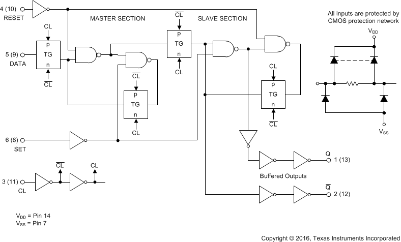
The CD4013B device consists of two identical, independent data-type flip-flops. Each flip-flop has independent data, set, reset, and clock inputs and Q and Q outputs. These devices can be used for shift register applications, and, by connecting Q output to the data input, for counter and toggle applications. The logic level present at the D input is transferred to the Q output during the positive-going transition of the clock pulse. Setting or resetting is independent of the clock and is accomplished by a high level on the set or reset line, respectively.
The CD4013B types are supplied in 14-pin dual-in-line plastic packages (E suffix), 14-pin small-outline packages (M, MT, M96, and NSR suffixes), and
14-pin thin shrink small-outline packages (PW and PWR suffixes).
Device Information(1)
| PART NUMBER | PACKAGE | BODY SIZE (NOM) |
|---|---|---|
| CD4013BE | PDIP (14) | 19.30 mm x 6.35 mm |
| CD4013BF | CDIP (14) | 19.50 mm x 6.92 mm |
| CD4013BM | SOIC (14) | 8.65 mm x 3.90 mm |
| CD4013BNS | SO (14) | 10.20 mm x 5.30 mm |
| CD4013BPW | TSSOP (14) | 5.00 mm x 4.40 mm |
- For all available packages, see the orderable addendum at the end of the data sheet.
Logic Diagram
