SNAS787A November 2019 – February 2020 CDCDB2000
PRODUCTION DATA.
- 1 Features
- 2 Applications
- 3 Description
- 4 Revision History
- 5 Pin Configuration and Functions
- 6 Specifications
-
7 Detailed Description
- 7.1 Overview
- 7.2 Functional Block Diagram
- 7.3 Feature Description
- 7.4 Device Functional Modes
- 7.5 Programming
- 7.6
Register Maps
- 7.6.1
CDCDB2000 Registers
- 7.6.1.1 OECR1 Register (Address = 0h) [reset = 78h]
- 7.6.1.2 OECR2 Register (Address = 1h) [reset = FFh]
- 7.6.1.3 OECR3 Register (Address = 2h) [reset = FFh]
- 7.6.1.4 OERDBK Register (Address = 3h) [reset = 0h]
- 7.6.1.5 SBRDBK Register (Address = 4h) [reset = 1h]
- 7.6.1.6 VDRREVID Register (Address = 5h) [reset = X]
- 7.6.1.7 DEVID Register (Address = 6h) [reset = X]
- 7.6.1.8 BTRDCNT Register (Address = 7h) [reset = 8h]
- 7.6.1.9 SBIMSK1 Register (Address = 8h) [reset = 0h]
- 7.6.1.10 SBIMSK2 Register (Address = 9h) [reset = 0h]
- 7.6.1.11 SBIMSK3 Register (Address = Ah) [reset = 0h]
- 7.6.1
CDCDB2000 Registers
- 8 Application and Implementation
- 9 Power Supply Recommendations
- 10Layout
- 11Device and Documentation Support
- 12Mechanical, Packaging, and Orderable Information
Package Options
Mechanical Data (Package|Pins)
- NPP|80
Thermal pad, mechanical data (Package|Pins)
Orderable Information
10.2 Layout Examples
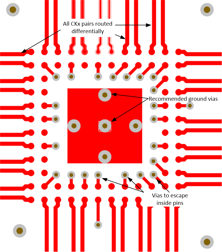
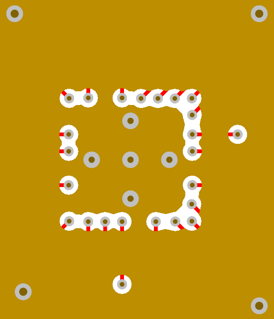
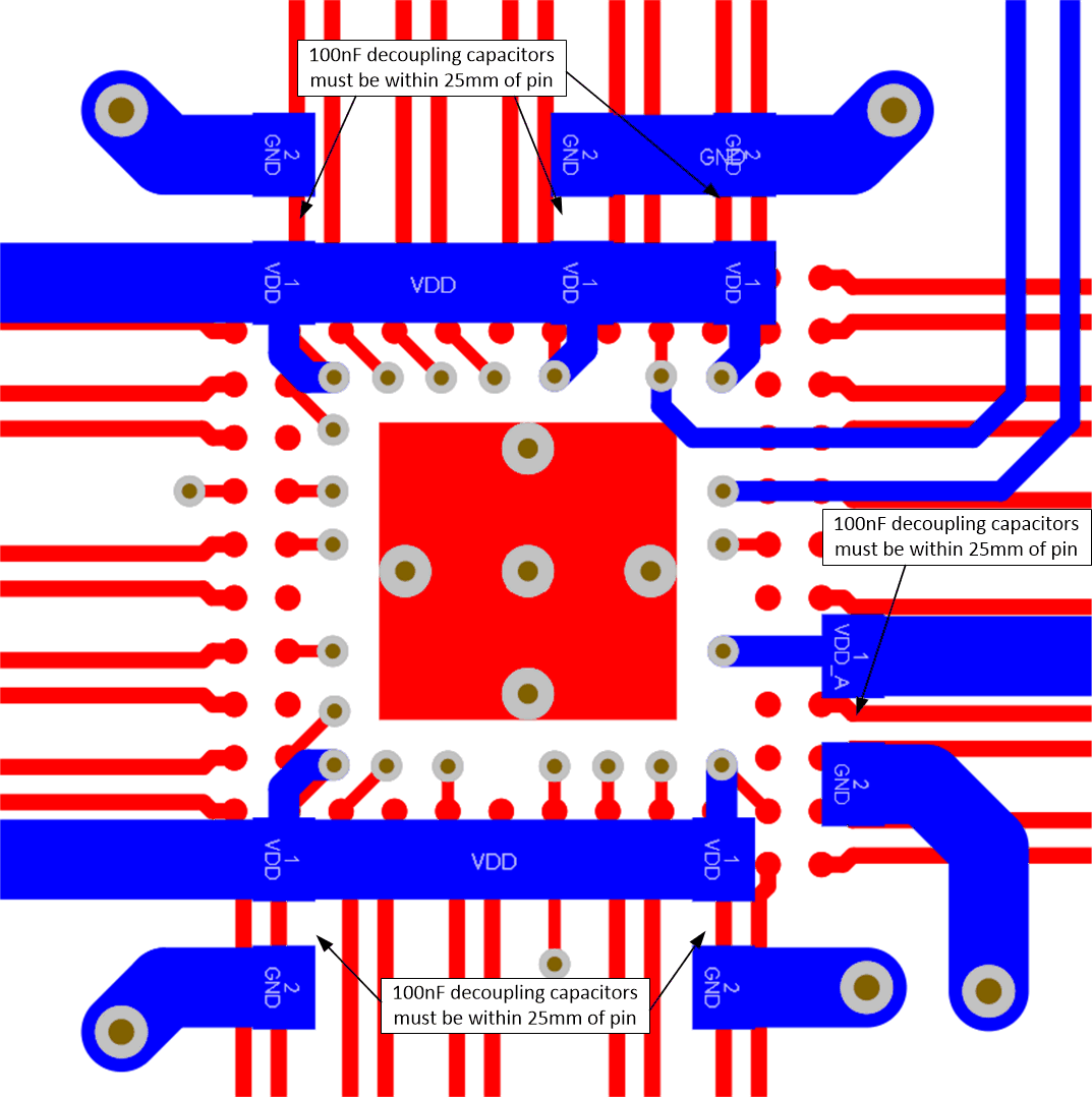
Figure 12 and Figure 13 are PCB layout examples that show the application of thermal design practices and a low-inductance ground connection between the device DAP and the PCB.
The CDCDB2000 has 85-Ω differential output impedance LP-HCSL format drivers. All transmission lines connected to CKx pins should be 85-Ω differential impedance, 42.5-Ω single-ended impedance to avoid reflections and increased radiated emissions. Take care to eliminate or reduce stubs on the transmission lines.
 Figure 12. PCB Layout Example for CDCDB2000, Top Layer
  Figure 13. PCB Layout Example for CDCDB2000, GND Layer
  Figure 14. PCB Layout Example for CDCDB2000, Bottom Layer