SNAS787A November 2019 – February 2020 CDCDB2000
PRODUCTION DATA.
- 1 Features
- 2 Applications
- 3 Description
- 4 Revision History
- 5 Pin Configuration and Functions
- 6 Specifications
-
7 Detailed Description
- 7.1 Overview
- 7.2 Functional Block Diagram
- 7.3 Feature Description
- 7.4 Device Functional Modes
- 7.5 Programming
- 7.6
Register Maps
- 7.6.1
CDCDB2000 Registers
- 7.6.1.1 OECR1 Register (Address = 0h) [reset = 78h]
- 7.6.1.2 OECR2 Register (Address = 1h) [reset = FFh]
- 7.6.1.3 OECR3 Register (Address = 2h) [reset = FFh]
- 7.6.1.4 OERDBK Register (Address = 3h) [reset = 0h]
- 7.6.1.5 SBRDBK Register (Address = 4h) [reset = 1h]
- 7.6.1.6 VDRREVID Register (Address = 5h) [reset = X]
- 7.6.1.7 DEVID Register (Address = 6h) [reset = X]
- 7.6.1.8 BTRDCNT Register (Address = 7h) [reset = 8h]
- 7.6.1.9 SBIMSK1 Register (Address = 8h) [reset = 0h]
- 7.6.1.10 SBIMSK2 Register (Address = 9h) [reset = 0h]
- 7.6.1.11 SBIMSK3 Register (Address = Ah) [reset = 0h]
- 7.6.1
CDCDB2000 Registers
- 8 Application and Implementation
- 9 Power Supply Recommendations
- 10Layout
- 11Device and Documentation Support
- 12Mechanical, Packaging, and Orderable Information
Package Options
Mechanical Data (Package|Pins)
- NPP|80
Thermal pad, mechanical data (Package|Pins)
Orderable Information
7.5 Programming
The CDCDB2000 has two methods to program the states of its 20 output drivers: SMBus and SBI.
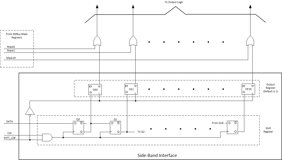
To select between SMBus and SBI interfaces, the SBEN pin is used. Pulling the SBEN to a high level enables the SBI. Pulling the SBEN pin to ground enables the SMBus interface. When SBI is enabled, the SMBus Mask registers are active. The SMBus Mask registers allow the function of the SBI shift registers to be disabled and set the each individual channel as enabled. See Figure 7 for a diagram of how the SMBus Mask registers and SBI shift register interact to enable or disable each output.
 Figure 7. SMBus Mask Register and SBI Shift Register Logic