SNAS787A November 2019 – February 2020 CDCDB2000
PRODUCTION DATA.
- 1 Features
- 2 Applications
- 3 Description
- 4 Revision History
- 5 Pin Configuration and Functions
- 6 Specifications
-
7 Detailed Description
- 7.1 Overview
- 7.2 Functional Block Diagram
- 7.3 Feature Description
- 7.4 Device Functional Modes
- 7.5 Programming
- 7.6
Register Maps
- 7.6.1
CDCDB2000 Registers
- 7.6.1.1 OECR1 Register (Address = 0h) [reset = 78h]
- 7.6.1.2 OECR2 Register (Address = 1h) [reset = FFh]
- 7.6.1.3 OECR3 Register (Address = 2h) [reset = FFh]
- 7.6.1.4 OERDBK Register (Address = 3h) [reset = 0h]
- 7.6.1.5 SBRDBK Register (Address = 4h) [reset = 1h]
- 7.6.1.6 VDRREVID Register (Address = 5h) [reset = X]
- 7.6.1.7 DEVID Register (Address = 6h) [reset = X]
- 7.6.1.8 BTRDCNT Register (Address = 7h) [reset = 8h]
- 7.6.1.9 SBIMSK1 Register (Address = 8h) [reset = 0h]
- 7.6.1.10 SBIMSK2 Register (Address = 9h) [reset = 0h]
- 7.6.1.11 SBIMSK3 Register (Address = Ah) [reset = 0h]
- 7.6.1
CDCDB2000 Registers
- 8 Application and Implementation
- 9 Power Supply Recommendations
- 10Layout
- 11Device and Documentation Support
- 12Mechanical, Packaging, and Orderable Information
Package Options
Mechanical Data (Package|Pins)
- NPP|80
Thermal pad, mechanical data (Package|Pins)
Orderable Information
7.5.2 SBI
Side-Band Interface (SBI) is a simple 3-wire serial interface. This interface consists of DATA, CLK and SHFT_LD# pins. When the SHFT_LD# pin is high, the rising edge of CLK clocks DATA into a shift register. After shifting data, the falling edge of SHFT_LD# loads the shift register contents into the Output Register. Both the SBI and the traditional SMBus interface feed common output enable/disable synchronization logic, which ensures glitch-free enable and disable outputs regardless of the method used.
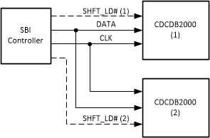
SBI can be configured at a system level in three ways: star topology, daisy chain topology, and directly. The star topology is shown in Figure 8. The daisy chain topology is shown in Figure 9.
 Figure 8. SBI Star Topology
  Figure 9. SBI Daisy Chain Topology