SCAS847I July 2007 – October 2016 CDCE925 , CDCEL925
PRODUCTION DATA.
- 1 Features
- 2 Applications
- 3 Description
- 4 Revision History
- 5 Description (continued)
- 6 Pin Configuration and Functions
- 7 Specifications
- 8 Parameter Measurement Information
- 9 Detailed Description
- 10Application and Implementation
- 11Power Supply Recommendations
- 12Layout
- 13Device and Documentation Support
- 14Mechanical, Packaging, and Orderable Information
Package Options
Mechanical Data (Package|Pins)
- PW|16
Thermal pad, mechanical data (Package|Pins)
Orderable Information
10 Application and Implementation
NOTE
Information in the following applications sections is not part of the TI component specification, and TI does not warrant its accuracy or completeness. TI’s customers are responsible for determining suitability of components for their purposes. Customers should validate and test their design implementation to confirm system functionality.
10.1 Application Information
The CDCEx925 device is an easy-to-use high-performance, programmable CMOS clock synthesizer. it can be used as a crystal buffer, clock synthesizer with separate output supply pin. The CDCEx925 features an on-chip loop filter and Spread-spectrum modulation. Programming can be done through SPI, pin-mode, or using on-chip EEPROM. This section shows some examples of using CDCEx925 in various applications.
10.2 Typical Application
Figure 15 shows the use of the CDCEx925 devices for replacement of crystals and crystal oscillators on a Gigabit Ethernet Switch application.
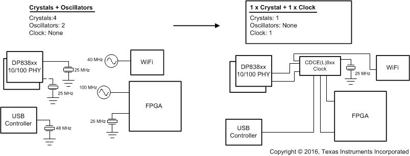 Figure 15. Crystal and Oscillator Replacement Example
10.2.1 Design Requirements
CDCEx925 supports spread spectrum clocking (SSC) with multiple control parameters:
- Modulation amount (%)
- Modulation frequency (>20 kHz)
- Modulation shape (triangular)
- Center spread / down spread (± or –)
 Figure 16. Modulation Frequency (fm) and Modulation Amount
10.2.2 Detailed Design Procedure
10.2.2.1 Spread Spectrum Clock (SSC)
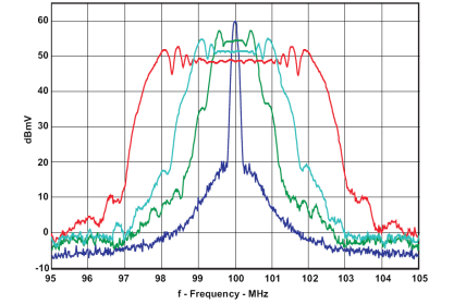
Spread spectrum modulation is a method to spread emitted energy over a larger bandwidth. In clocking, spread spectrum can reduce Electromagnetic Interference (EMI) by reducing the level of emission from clock distribution network.
10.2.2.2 PLL Multiplier/Divider Definition
At a given input frequency (ƒIN), the output frequency (ƒOUT) of the CDCEx925 is calculated with Equation 1.

where
- M (1 to 511) and N (1 to 4095) are the multiplier/divide values of the PLL
- Pdiv (1 to 127) is the output divider
The target VCO frequency (ƒVCO) of each PLL is calculated with Equation 2.

The PLL internally operates as fractional divider and needs the following multiplier/divider settings:

where
- N′ = N × 2P
- N ≥ M
- 80 MHz ≤ ƒVCO ≤ 230 MHz
- 16 ≤ q ≤ 63
- 0 ≤ p ≤ 4
- 0 ≤ r ≤ 511
| Example: | |||
| for ƒIN = 27 MHz; M = 1; N = 4; Pdiv = 2; | for ƒIN = 27 MHz; M = 2; N = 11; Pdiv = 2; | ||
| → | fOUT = 54 MHz | → | fOUT = 74.25 MHz |
| → | fVCO = 108 MHz | → | fVCO = 148.50 MHz |
| → | P = 4 – int(log24) = 4 – 2 = 2 | → | P = 4 – int(log25.5) = 4 – 2 = 2 |
| → | N′’ = 4 × 22 = 16 | → | N′’ = 11 × 22 = 44 |
| → | Q = int(16) = 16 | → | Q = int(22) = 22 |
| → | R = 16 – 16 = 0 | → | R = 44 – 44 = 0 |
The values for P, Q, R, and N’ are automatically calculated when using TI Pro-Clock™ software.
10.2.2.3 Crystal Oscillator Start-Up
When the CDCEx925 is used as a crystal buffer, crystal oscillator start-up dominates the start-up time compared to the internal PLL lock time. The following diagram shows the oscillator start-up sequence for a 27-MHz crystal input with an 8-pF load. The start-up time for the crystal is in the order of approximately 250 µs compared to approximately 10 µs of lock time. In general, lock time is an order of magnitude less compared to the crystal start-up time.
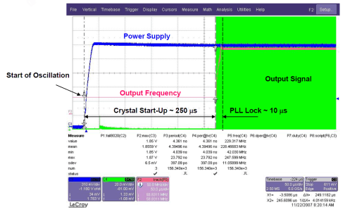 Figure 18. Crystal Oscillator Start-Up vs PLL Lock Time
10.2.2.4 Frequency Adjustment With Crystal Oscillator Pulling
The frequency for the CDCEx925 is adjusted for media and other applications with the VCXO control input VCtrl. If a PWM modulated signal is used as a control signal for the VCXO, an external filter is needed.
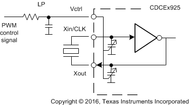 Figure 19. Frequency Adjustment Using PWM Input to the VCXO Control
10.2.2.5 Unused Inputs and Outputs
If VCXO pulling functionality is not required, VCtrl should be left floating. All other unused inputs should be set to GND. Unused outputs should be left floating.
If one output block is not used, TI recommends disabling it. However, TI always recommends providing the supply for the second output block even if it is disabled.
10.2.2.6 Switching Between XO and VCXO Mode
When the CDCEx925 is in crystal oscillator or in VCXO configuration, the internal capacitors require different internal capacitance. The following steps are recommended to switch to VCXO mode when the configuration for the on-chip capacitor is still set for XO mode. To center the output frequency to 0 ppm:
- While in XO mode, put Vctrl = Vdd/2
- Switch from X0 mode to VCXO mode
- Program the internal capacitors to obtain 0 ppm at the output.
10.2.3 Application Curves
Figure 20, Figure 21, Figure 22, and Figure 23 show CDCEx925 measurements with the SSC feature enabled. Device configuration: 27-MHz input, 27-MHz output.
 Figure 20. fOUT = 27 MHz, VCO Frequency < 125 MHz, SSC (2% Center)
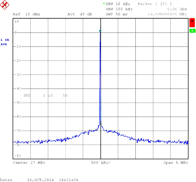 Figure 22. Output Spectrum With SSC Off
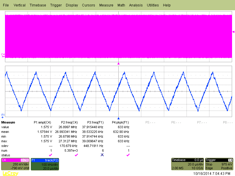 Figure 21. fOUT = 27 MHz, VCO Frequency > 175 MHz, SSC (1%, Center)
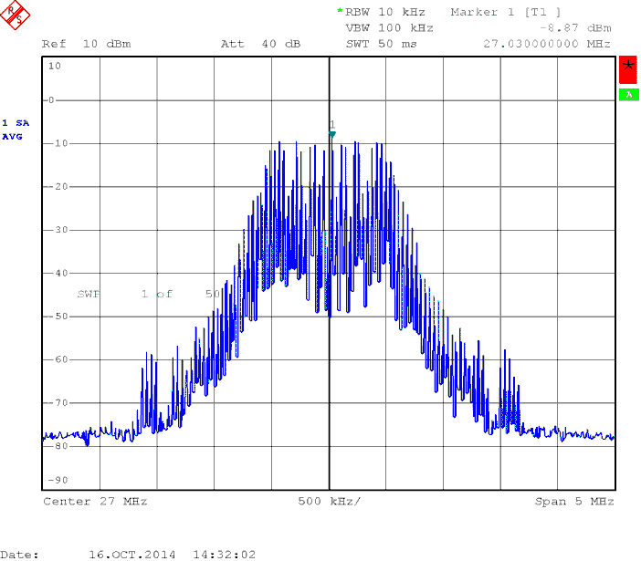 Figure 23. Output Spectrum With SSC On, 2% Center