SCAS946A November 2016 – January 2017 CDCLVP111-SP
PRODUCTION DATA.
- 1 Features
- 2 Applications
- 3 Description
- 4 Revision History
- 5 Pin Configuration and Functions
- 6 Specifications
- 7 Detailed Description
- 8 Application and Implementation
- 9 Power Supply Recommendations
- 10Layout
- 11Device and Documentation Support
- 12Mechanical, Packaging, and Orderable Information
Package Options
Refer to the PDF data sheet for device specific package drawings
Mechanical Data (Package|Pins)
- HFG|36
Thermal pad, mechanical data (Package|Pins)
Orderable Information
1 Features
- Distributes One Differential Clock Input Pair LVPECL to 10 Differential LVPECL
- Fully Compatible With LVECL and LVPECL
- Supports a Wide Supply Voltage Range From 2.375 V to 3.8 V
- Selectable Clock Input Through CLK_SEL
- Low-Output Skew (Typical 15 ps) for Clock-Distribution Applications
- Additive Jitter Less Than 1 ps
- Propagation Delay Less Than 355 ps
- Open Input Default State
- LVDS, CML, SSTL input Compatible
- VBB Reference Voltage Output for Single-Ended Clocking
- Frequency Range From DC to 3.5 GHz
-
Supports Defense, Aerospace, and Medical Applications
- Controlled Baseline
- One Assembly and Test Site
- One Fabrication Site
- Available in Military (–55°C to 125°C) Temperature Range (1)
- Extended Product Life Cycle
- Extended Product-Change Notification
- Product Traceability
2 Applications
- Designed for Driving 50-Ω Transmission Lines
- High-Performance Clock Distribution
- Engineering Evaluation (/EM) Samples Are Available (1)
3 Description
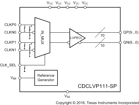
The CDCLVP111-SP clock driver distributes one differential clock pair of LVPECL input, (CLK0, CLK1) to ten pairs of differential LVPECL clock (Q0, Q9) outputs with minimum skew for clock distribution. The CDCLVP111-SP can accept two clock sources into an input multiplexer. The CDCLVP111-SP is specifically designed for driving 50-Ω transmission lines. When an output pin is not used, leaving it open is recommended to reduce power consumption. If only one of the output pins from a differential pair is used, the other output pin must be identically terminated to 50 Ω.
The VBB reference voltage output is used if single-ended input operation is required. In this case, the VBB pin should be connected to CLK0 and bypassed to GND via a 10-nF capacitor.
For high-speed performance, the differential mode is strongly recommended.
The CDCLVP111-SP is characterized for operation from –55°C to 125°C.
Device Information(1)
| PART NUMBER | PACKAGE | BODY SIZE (NOM) |
|---|---|---|
| CDCLVP111-SP | HFG (36) | 9.08 mm × 9.08 mm |
- For all available packages, see the orderable addendum at the end of the data sheet.
Functional Block Diagram
