SCAS880F August 2009 – September 2015 CDCLVP1204
PRODUCTION DATA.
- 1 Features
- 2 Applications
- 3 Description
- 4 Revision History
- 5 Pin Configuration and Functions
-
6 Specifications
- 6.1 Absolute Maximum Ratings
- 6.2 ESD Ratings
- 6.3 Recommended Operating Conditions
- 6.4 Thermal Information
- 6.5 Terminal Characteristics
- 6.6 Electrical Characteristics: LVCMOS Input
- 6.7 Electrical Characteristics: Differential Input
- 6.8 Electrical Characteristics: LVPECL Output
- 6.9 Electrical Characteristics: LVPECL Output
- 6.10 Timing Diagrams
- 6.11 Typical Characteristics
- 7 Parameter Measurement Information
- 8 Detailed Description
- 9 Applications and Implementation
- 10Power Supply Recommendations
- 11Layout
- 12Device and Documentation Support
- 13Mechanical, Packaging, and Orderable Information
Package Options
Mechanical Data (Package|Pins)
- RGT|16
Thermal pad, mechanical data (Package|Pins)
- RGT|16
Orderable Information
9 Applications and Implementation
NOTE
Information in the following applications sections is not part of the TI component specification, and TI does not warrant its accuracy or completeness. TI’s customers are responsible for determining suitability of components for their purposes. Customers should validate and test their design implementation to confirm system functionality.
9.1 Application Information
The CDCLVP1204 is a low additive jitter LVPECL fanout buffer that can generate four copies of two selectable LVPECL, LVDS, or LVCMOS inputs. The CDCLVP1204 can accept reference clock frequencies up to 2 GHz while providing low output skew.
9.2 Typical Application
9.2.1 Fanout Buffer for Line Card Application
9.2.1.1 Design Requirements
The CDCLVP1204 shown in Figure 20 is configured to be able to select two inputs, a 156.25-MHz LVPECL clock from the backplane, or a secondary 156.25-MHz LVCMOS 2.5-V oscillator. Either signal can be then fanned out to desired devices, as shown.
The configuration example is driving 4 LVPECL receivers in a line card application with the following properties:
- The PHY device has internal AC coupling and appropriate termination and biasing. The CDCLVP1204 will need to be provided with 86-Ω emitter resistors near the driver for proper operation.
- The ASIC is capable of DC coupling with a 2.5-V LVPECL driver such as the CDCLVP1204. This ASIC features internal termination so no additional components are needed.
- The FPGA requires external AC coupling but has internal termination. Again, 86-Ω emitter resistors are placed near the CDCLVP1204 and 0.1 µF are placed to provide AC coupling. Similarly, the CPU is internally terminated and requires external AC coupling capacitors.
9.2.1.2 Detailed Design Procedure
Refer to Input Termination for proper input terminations, dependent on single ended or differential inputs.
Refer to LVPECL Output Termination for output termination schemes depending on the receiver application.
Unused outputs can be left floating.
In this example, the PHY, ASIC, and FPGA/CPU require different schemes. Power supply filtering and bypassing is critical for low noise applications.
See Power Supply Recommendations for recommended filtering techniques. A reference layout is provided on the CDCLVP1204 Evaluation Module at SCAU032.
9.2.1.3 Application Curves

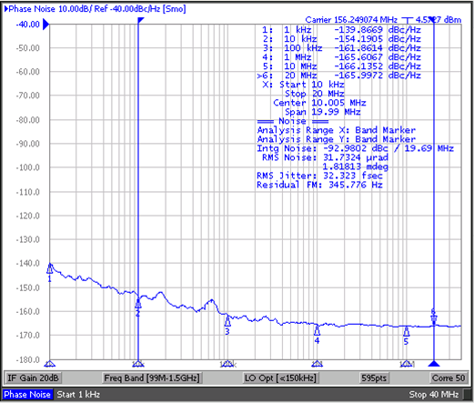
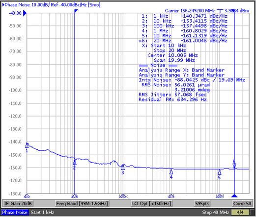
| Reference signal is low noise Crystek XO CPRO33.156.25 | ||
(10 kHz to 20 MHz)

(10 kHz to 20 MHz)
The CDCLVP12xx's low additive noise can be shown in this line card application. The low noise 156.25 MHz XO with 32 fs RMS jitter drives the CDCLVP12xx, resulting in 57 fs RMS when integrated from 10 kHz to 20 MHz. The resultant additive jitter is a low 47 fs RMS for this configuration.