SLPS313A September 2013 – January 2018 CSD13202Q2
PRODUCTION DATA.
- 1Features
- 2Applications
- 3Description
- 4Revision History
- 5Specifications
- 6Device and Documentation Support
- 7Mechanical, Packaging, and Orderable Information
Package Options
Refer to the PDF data sheet for device specific package drawings
Mechanical Data (Package|Pins)
- DQK|6
Thermal pad, mechanical data (Package|Pins)
Orderable Information
5.2 Thermal Characteristics
TA = 25°C unless otherwise stated| PARAMETER | MIN | TYP | MAX | UNIT | |
|---|---|---|---|---|---|
| RθJC | Thermal resistance junction-to-case(1) | 6.4 | °C/W | ||
| RθJA | Thermal resistance junction-to-ambient(1)(2) | 60 | °C/W | ||
(1) RθJC is determined with the device mounted on a 1-in2 (6.45-cm2), 2-oz (0.071-mm) thick Cu pad on a 1.5-in × 1.5-in (3.81-cm × 3.81-cm), 0.06-in (1.52-mm) thick FR4 PCB. RθJC is specified by design, whereas RθJA is determined by the user’s board design.
(2) Device mounted on FR4 material with 1-in2 (6.45-cm2), 2-oz (0.071-mm) thick Cu.
 |
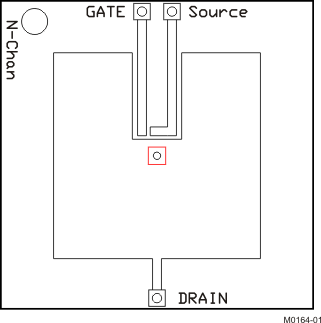
Max RθJA = 60 when mounted on 1 in2 (6.45 cm2) of 2-oz (0.071-mm) thick Cu. |  |
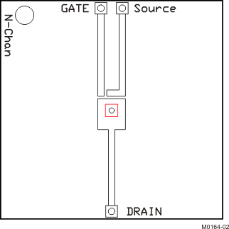
Max RθJA = 210 when mounted on minimum pad area of 2-oz (0.071-mm) thick Cu. |