SLPS508A June 2014 – July 2014 CSD25202W15
PRODUCTION DATA.
- 1Features
- 2Applications
- 3Description
- 4Revision History
- 5Specifications
- 6Device and Documentation Support
- 7Mechanical, Packaging, and Orderable Information
Package Options
Refer to the PDF data sheet for device specific package drawings
Mechanical Data (Package|Pins)
- YZF|9
Thermal pad, mechanical data (Package|Pins)
Orderable Information
1 Features
- Low-Resistance
- Small Footprint 1.5 mm × 1.5 mm
- Gate ESD Protection –3 kV
- Pb Free
- RoHS Compliant
- Halogen Free
- Gate-Source Voltage Clamp
2 Applications
- Battery Management
- Battery Protection
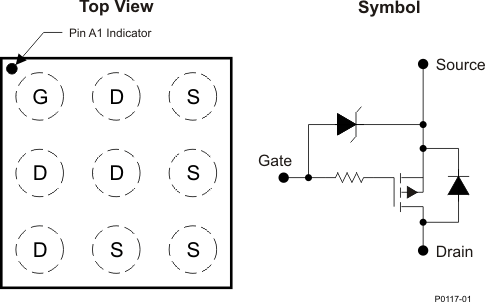
3 Description
This 21 mΩ, 20 V device is designed to deliver the lowest on resistance and gate charge in a small 1.5 mm × 1.5 mm chip scale package with excellent thermal characteristics in an ultra-low profile. Low on resistance coupled with the small footprint and low profile make the device ideal for battery operated space constrained applications.
Product Summary
Ordering Information(1)
| Device | Qty | Media | Package | Ship |
|---|---|---|---|---|
| CSD25202W15 | 3000 | 7-Inch Reel | 1.5-mm × 1.5-mm Wafer Level Package | Tape and Reel |
| CSD25202W15T | 250 | 7-Inch Reel |
- For all available packages, see the orderable addendum at the end of the data sheet.
Absolute Maximum Ratings
| TA = 25°C | VALUE | UNIT | |
|---|---|---|---|
| VDS | Drain-to-Source Voltage | –20 | V |
| VGS | Gate-to-Source Voltage | –6 | V |
| ID | Continuous Drain Current(1) | –4 | A |
| Pulsed Drain Current(2) | –38 | A | |
| IG | Continuous Gate Current(1) | –0.5 | A |
| Pulsed Gate Current(2) | –7 | A | |
| PD | Power Dissipation | 0.5 | W |
| TJ, Tstg |
Operating Junction and Storage Temperature Range |
–55 to 150 | °C |
- Ball limited
- Typical RθJA = 220ºC/W, pulse duration ≤100 µs, duty cycle ≤ 1%
RDS(on) vs VGS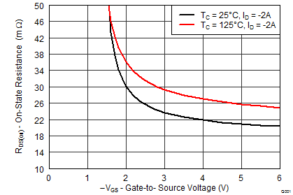 |
Gate Charge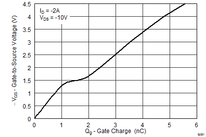 |