SLPS523B February 2015 – May 2019 CSD87501L
PRODUCTION DATA.
- 1Features
- 2Applications
- 3Description
- 4Revision History
- 5Specifications
- 6Device and Documentation Support
- 7Mechanical, Packaging, and Orderable Information
Package Options
Refer to the PDF data sheet for device specific package drawings
Mechanical Data (Package|Pins)
- YJG|10
Thermal pad, mechanical data (Package|Pins)
Orderable Information
3 Description
This 30-V, 6.6-mΩ, 3.37-mm × 1.47-mm LGA Dual NexFET™ power MOSFET is designed to minimize resistance and gate charge in a small footprint. Its small size and common drain configuration make the device ideal for multi-cell battery pack applications and small handheld devices.
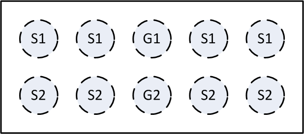
Top View

Configuration

Product Summary
| TA = 25°C | TYPICAL VALUE | UNIT | ||
|---|---|---|---|---|
| VS1S2 | Source-to-Source Voltage | 30 | V | |
| Qg | Gate Charge Total (4.5 V) | 15 | nC | |
| Qgd | Gate Charge Gate-to-Drain | 6.0 | nC | |
| RS1S2(on) | Source-to-Source On-Resistance | VGS = 4.5 V | 9.3 | mΩ |
| VGS = 10 V | 6.6 | |||
| VGS(th) | Threshold Voltage | 1.8 | V | |
Device Information(1)
| DEVICE | MEDIA | QTY | PACKAGE | SHIP |
|---|---|---|---|---|
| CSD87501L | 7-Inch Reel | 3000 | 3.37 mm × 1.47 mm
Land Grid Array Package |
Tape
and Reel |
| CSD87501LT | 7-Inch Reel | 250 |
- For all available packages, see the orderable addendum at the end of the data sheet.
Absolute Maximum Ratings
| TA = 25°C | VALUE | UNIT | |
|---|---|---|---|
| VS1S2 | Source-to-Source Voltage | 30 | V |
| VGS | Gate-to-Source Voltage | ±20 | V |
| IS | Continuous Source Current(1) | 14 | A |
| ISM | Pulsed Source Current(2) | 72 | A |
| PD | Power Dissipation | 2.5 | W |
| V(ESD) | Human-Body Model (HBM) | 2 | kV |
| TJ,
Tstg |
Operating Junction,
Storage Temperature |
–55 to 150 | °C |
- Typical RθJA = 50°C/W on a 1-in2, 2-oz Cu pad on a 0.06-in thick FR4 PCB.
- Typical min Cu RθJA = 135°C/W, pulse duration ≤ 100 μs, duty cycle ≤ 1%.