SLPS430A August 2013 – August 2014 CSD95375Q4M
PRODUCTION DATA.
- 1 Features
- 2 Applications
- 3 Description
- 4 Revision History
- 5 Pin Configuration
- 6 Specifications
- 7 Electrical Characteristics
- 8 Typical Characteristics
- 9 Detailed Description
- 10Application and Implementation
- 11Layout
- 12Device and Documentation Support
- 13Mechanical, Packaging, and Orderable Information
Package Options
Mechanical Data (Package|Pins)
- DPC|8
Thermal pad, mechanical data (Package|Pins)
Orderable Information
1 Features
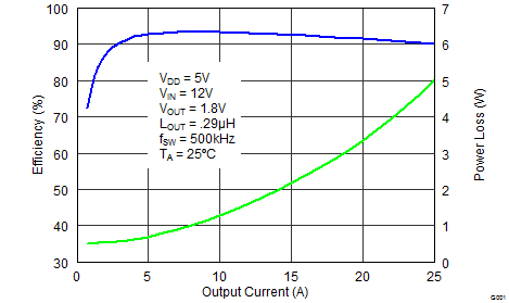
- 93% System Efficiency at 15 A
- Max Rated Continuous Current 25 A, Peak 60 A
- High Frequency Operation (up to 2 MHz)
- High Density - SON 3.5 × 4.5-mm Footprint
- Ultra-Low Inductance Package
- System Optimized PCB Footprint
- Ultra-Low Quiescent (ULQ) Current Mode
- 3.3 V and 5 V PWM Signal Compatible
- Diode Emulation Mode with FCCM
- Tri-State PWM Input
- Integrated Bootstrap Diode
- Shoot Through Protection
- RoHS Compliant – Lead-Free Terminal Plating
- Halogen Free
2 Applications
- Ultrabook/Notebook DC/DC Converters
- Multiphase Vcore and DDR Solutions
- Point of Load Synchronous Buck in Networking, Telecom, and Computing Systems
3 Description
The CSD95375Q4M NexFET™ Power Stage is a highly optimized design for use in a high power, high density Synchronous Buck converter. This product integrates the driver IC and NexFET technology to complete the power stage switching function. The driver IC has a built-in selectable diode emulation function that enables DCM operation to improve light load efficiency. In addition, the driver IC supports ULQ mode that enables Connected Standby for Windows™ 8. With the PWM input in tri-state, quiescent current is reduced to 130 µA, with immediate response. When SKIP# is held at tri-state, the current is reduced to 8 µA (typically 20 µs is required to resume switching). This combination produces a high current, high efficiency, and high speed switching device in a small 3.5 × 4.5-mm outline package. In addition, the PCB footprint has been optimized to help reduce design time and simplify the completion of the overall system design.
Device Information(1)
| Device | Media | Qty | Package | Ship |
|---|---|---|---|---|
| CSD95375Q4M | 13-Inch Reel | 2500 | SON 3.5 × 4.5 mm Plastic Package |
Tape and Reel |
| CSD95375Q4MT | 7-Inch Reel | 250 |
- For all available packages, see the orderable addendum at the end of the data sheet.
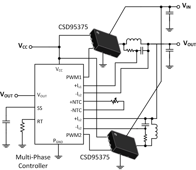
Application Diagram
Typical Power Stage Efficiency and Power Loss