SLPS714A January 2019 – March 2019 CSD96497Q5MC
PRODUCTION DATA.
- 1Features
- 2Applications
- 3Description
- 4Revision History
- 5Device and Documentation Support
- 6Mechanical, Packaging, and Orderable Information
- 7Package Option Addendum
Package Options
Mechanical Data (Package|Pins)
- DMC|12
Thermal pad, mechanical data (Package|Pins)
Orderable Information
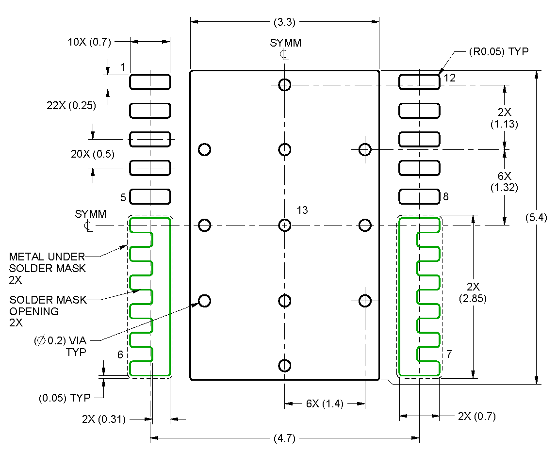
6.2 Recommended PCB Land Pattern


- All linear dimensions are in millimeters. Any dimensions in parenthesis are for reference only. Dimensioning and tolerancing per ASME Y14.5M.
- This drawing is subject to change without notice.
- This package is designed to be soldered to thermal pads on the board. For more information, see QFN/SON PCB Attachment (SLUA271).
- Vias are optional depending on application, refer to device data sheet. If any vias are implemented, refer to their locations shown on this view. It is recommended that vias under paste be filled, plugged or tented.