SNAS424D August 2007 – April 2016 DAC088S085
PRODUCTION DATA.
- 1 Features
- 2 Applications
- 3 Description
- 4 Revision History
- 5 Description (continued)
- 6 Pin Configuration and Functions
- 7 Specifications
- 8 Detailed Description
- 9 Application and Implementation
- 10Power Supply Recommendations
- 11Layout
- 12Device and Documentation Support
- 13Mechanical, Packaging, and Orderable Information
Package Options
Mechanical Data (Package|Pins)
Thermal pad, mechanical data (Package|Pins)
Orderable Information
1 Features
- Ensured Monotonicity
- Low Power Operation
- Rail-to-Rail Voltage Output
- Daisy Chain Capability
- Power-On Reset to 0 V
- Simultaneous Output Updating
- Individual Channel Power Down Capability
- Wide Power Supply Range (2.7 V to 5.5 V)
- Dual Reference Voltages With Range of 0.5 V to VA
- Operating Temperature Range of –40°C to 125°C
- Industry's Smallest Package
- Key Specifications
- Resolution: 8 Bits
- INL: ±0.5 LSB (Maximum)
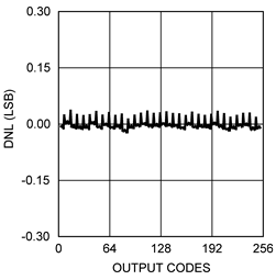
- DNL: 0.15 / –0.1 LSB (Maximum)
- Settling Time: 4.5 µs (Maximum)
- Zero Code Error: 15 mV (Maximum)
- Full-Scale Error: –0.75 %FSR (Maximum)
- Supply Power :
- Normal: 1.95 mW (3 V) / 4.85 mW (5 V) Typical
- Power Down: 0.3 µW (3 V) / 1 µW (5 V) Typical
2 Applications
- Battery-Powered Instruments
- Digital Gain and Offset Adjustment
- Programmable Voltage and Current Sources
- Programmable Attenuators
- Voltage Reference for ADCs
- Sensor Supply Voltage
- Range Detectors
3 Description
The DAC088S085 is a full-featured, general-purpose, OCTAL, 8-bit, voltage-output, digital-to-analog converter (DAC) that can operate from a single 2.7 V to 5.5 V supply and consumes 1.95 mW at 3 V and 4.85 mW at 5 V. The DAC088S085 is packaged in a 16-pin WQFN package and a 16-pin TSSOP package. The WQFN package makes the DAC088S085 the smallest OCTAL DAC in its class. The on-chip output amplifiers allow rail-to-rail output swing and the three-wire serial interface operates at clock rates up to 40 MHz over the entire supply voltage range. Competitive devices are limited to 25‑MHz clock rates at supply voltages in the range of 2.7 V to 3.6 V. The serial interface is compatible with standard SPI™, QSPI, MICROWIRE, and DSP interfaces. The DAC088S085 also offers daisy chain operation where an unlimited number of devices can be updated simultaneously using a single serial interface.
Device Information(1)
| PART NUMBER | PACKAGE | BODY SIZE (NOM) |
|---|---|---|
| DAC088S085 | TSSOP (16) | 5.00 mm × 4.40 mm |
| WQFN (16) | 4.00 mm × 4.00 mm |
- For all available packages, see the orderable addendum at the end of the data sheet.
DNL vs Code

4 Revision History
Changes from C Revision (March 2013) to D Revision
- Added ESD Ratings table, Feature Description section, Device Functional Modes, Application and Implementation section, Power Supply Recommendations section, Layout section, Device and Documentation Support section, and Mechanical, Packaging, and Orderable Information sectionGo
Changes from B Revision (March 2013) to C Revision
- Changed layout of National Data Sheet to TI formatGo