SNAS265J June 2005 – September 2015 DAC121S101 , DAC121S101-Q1
PRODUCTION DATA.
- 1 Features
- 2 Applications
- 3 Description
- 4 Revision History
- 5 Description continued
- 6 Pin Configuration and Functions
- 7 Specifications
- 8 Detailed Description
- 9 Application and Implementation
- 10Power Supply Recommendations
- 11Layout
- 12Device and Documentation Support
- 13Mechanical, Packaging, and Orderable Information
Package Options
Mechanical Data (Package|Pins)
Thermal pad, mechanical data (Package|Pins)
- DGK|8
Orderable Information
1 Features
- DAC121S101-Q1 is AEC-Q100 Grade 1 Qualified and is Manufactured on an Automotive Grade Flow.
- Ensured Monotonicity
- Low Power Operation
- Rail-to-Rail Voltage Output
- Power-on Reset to Zero Volts Output
- Wide Temperature Range of −40°C to +125°C
- Wide Power Supply Range of 2.7 V to 5.5 V
- Small Packages
- Power Down Feature
- Key Specifications
- 12-Bit Resolution
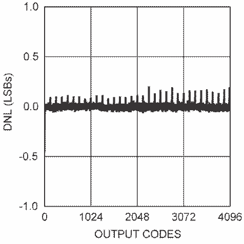
- DNL -0.15, +0.25 LSB (Typical)
- 8-µs Output Settling Time (Typical)
- 4-mV Zero Code Error (Typical)
- Full-Scale Error at −0.06 %FS (Typical)
- 0.64-mW (3.6-V) / 1.43-mW (5.5-V) Normal Mode Power Consumption (Typical)
- 0.14-µW (3.6-V) / 0.39-µW (5.5-V) Power-Down Mode (Typical)
2 Applications
- Battery-Powered Instruments
- Digital Gain and Offset Adjustment
- Programmable Voltage and Current Sources
- Programmable Attenuators
- Automotive
3 Description
The DAC121S101 device is a full-featured, general-purpose, 12-bit voltage-output digital-to-analog converter (DAC) that can operate from a single 2.7-V to 5.5-V supply and consumes just 177 µA of current at 3.6 V. The on-chip output amplifier allows rail-to-rail output swing and the three wire serial interface operates at clock rates up to 30 MHz over the specified supply voltage range and is compatible with standard SPI™, QSPI, MICROWIRE and DSP interfaces. Competitive devices are limited to 20-MHz clock rates at supply voltages in the 2.7 V to 3.6 V range.
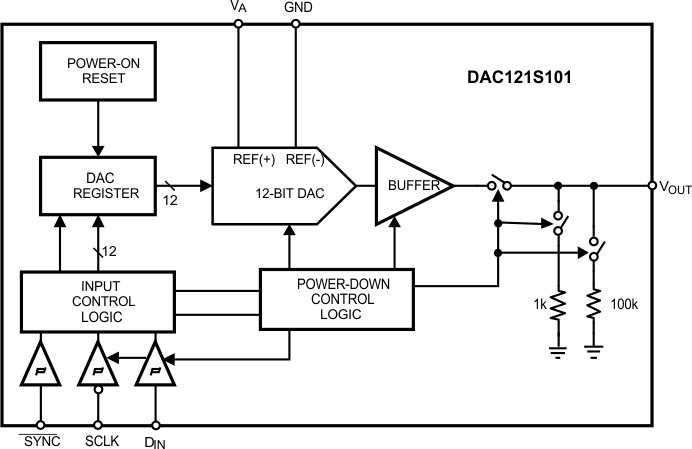
The supply voltage for the DAC121S101 serves as its voltage reference, providing the widest possible output dynamic range. A power-on reset circuit ensures that the DAC output powers up to zero volts and remains there until there is a valid write to the device. A power-down feature reduces power consumption to less than a microWatt.
The low power consumption and small packages of the DAC121S101 make it an excellent choice for use in battery operated equipment.
Device Information(1)
| PART NUMBER | PACKAGE | BODY SIZE (NOM) |
|---|---|---|
| DAC121S101 | SOT (6) | 2.90 mm × 1.60 mm |
| VSSOP (8) | 3.00 mm × 3.00 mm | |
| DAC121S101-Q1 | SOT (6) | 2.90 mm × 1.60 mm |
- For all available packages, see the orderable addendum at the end of the data sheet.
Simplified Block Diagram

DNL vs. Output Code
