SNAS515G July 2011 – December 2014 DAC161P997
PRODUCTION DATA.
- 1 Features
- 2 Application
- 3 Description
- 4 Revision History
- 5 Pin Configuration and Functions
- 6 Specifications
- 7 Detailed Description
- 8 Application and Implementation
- 9 Power Supply Recommendations
- 10Layout
- 11Device and Documentation Support
- 12Mechanical, Packaging, and Orderable Information
Package Options
Mechanical Data (Package|Pins)
- RGH|16
Thermal pad, mechanical data (Package|Pins)
Orderable Information
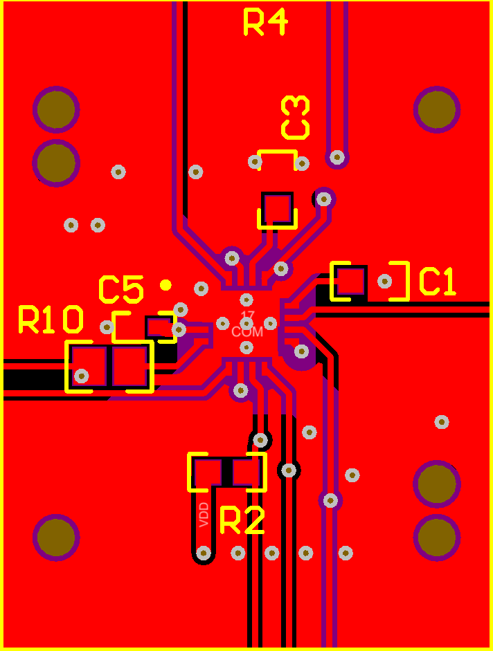
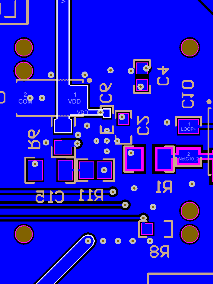
10 Layout
10.1 Layout Guidelines
To maximize the performance of the DAC161S997 in any application, good layout practices and proper circuit design must be followed. A few recommendations specific to the DAC161S997 are:
- Make sure that VD and VA have decoupling capacitors local to the respective terminals.
- Minimize trace length between the C1, C2, and C3 capacitors and the DAC161S997 pins.