SLAS837B April 2013 – January 2017 DAC3174
PRODUCTION DATA.
- 1 Features
- 2 Applications
- 3 Description
- 4 Revision History
- 5 Pin Configuration and Functions
-
6 Specifications
- 6.1 Absolute Maximum Ratings
- 6.2 ESD Ratings
- 6.3 Recommended Operating Conditions
- 6.4 Thermal Information
- 6.5 Electrical Characteristics: DC Specifications
- 6.6 Electrical Characteristics: AC Specifications
- 6.7 Electrical Characteristics: Digital Specifications
- 6.8 Timing Requirements
- 6.9 Typical Characteristics
-
7 Detailed Description
- 7.1 Overview
- 7.2 Functional Block Diagrams
- 7.3 Feature Description
- 7.4 Device Functional Modes
- 7.5 Programming
- 7.6
Register Maps
- 7.6.1 config0 Register (address = 0x00) [reset = 0x44FC]
- 7.6.2 config 1 Register (address = 0x01) [reset = 0x600E]
- 7.6.3 config2 Register (address = 0x02) [reset = 0x3FFF]
- 7.6.4 config3 Register (address = 0x03) [reset = 0x0000]
- 7.6.5 config4 Register (address = 0x04) [reset = 0x0000]
- 7.6.6 config5 Register (address = 0x05) [reset = 0x0000]
- 7.6.7 config6 Register (address = 0x06) [reset = 0x0000]
- 7.6.8 config7 Register (address = 0x07) [reset = 0xFFFF]
- 7.6.9 config8 Register (address = 0x08) [reset = 0x4000]
- 7.6.10 config9 Register (address = 0x09) [reset = 0x8000]
- 7.6.11 config10 Register (address = 0x0A) [reset = 0xF080]
- 7.6.12 config11 Register (address = 0x0B) [reset = 0x1111]
- 7.6.13 config12 Register (address = 0x0C) [reset = 0x3A7A]
- 7.6.14 config13 Register (address = 0x0D) [reset = 0x36B6]
- 7.6.15 config14 Register (address = 0x0E) [reset = 0x2AEA]
- 7.6.16 config15 Register (address = 0x0F) [reset = 0x0545]
- 7.6.17 config16 Register (address = 0x10) [reset = 0x0585]
- 7.6.18 config17 Register (address = 0x11) [reset = 0x0949]
- 7.6.19 config18 Register (address = 0x12) [reset = 0x1515]
- 7.6.20 config19 Register (address = 0x13) [reset = 0x3ABA]
- 7.6.21 config20 Register (address = 0x14) [reset = 0x0000]
- 7.6.22 config21 Register (address = 0x15) [reset = 0xFFFF]
- 7.6.23 config22 Register (address = 0x16) [reset = N/A]
- 7.6.24 config23 Register (address = 0x17) [reset = N/A]
- 7.6.25 config24 Register (address = 0x18) [reset = N/A]
- 7.6.26 config25 Register (address = 0x19) [reset = N/A]
- 7.6.27 config127 Register (address = 0x7F) [reset = 0x0045]
- 8 Application and Implementation
- 9 Power Supply Recommendations
- 10Layout
- 11Device and Documentation Support
- 12Mechanical, Packaging, and Orderable Information
Package Options
Mechanical Data (Package|Pins)
- RGC|64
Thermal pad, mechanical data (Package|Pins)
- RGC|64
Orderable Information
8 Application and Implementation
NOTE
Information in the following applications sections is not part of the TI component specification, and TI does not warrant its accuracy or completeness. TI’s customers are responsible for determining suitability of components for their purposes. Customers should validate and test their design implementation to confirm system functionality.
8.1 Application Information
The DAC3174 is a single-channel, 14-bit, 500-MSPS DAC with a flexible input interface (full SDR, 14-bit interface; or DDR, 7-bit interface). DAC3174 supports independent input data clock and output DAC clock, and the FIFO can be used to absorb the timing difference of two clock domains. The DAC3174 can be widely used in many applications, such as real-IF transmitter for wireless infrastructure, arbitrary waveform generator, radar, cable head-end equipment, and so on.
8.2 Typical Application
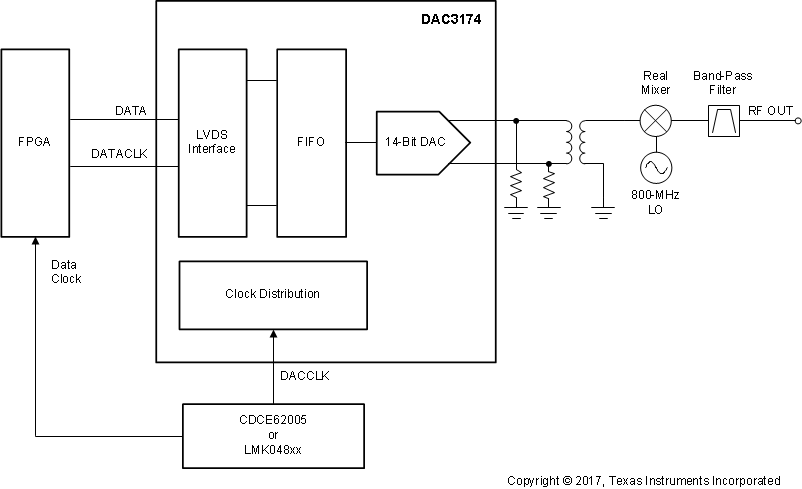
Figure 56 below shows an example block diagram of the DAC3174 used as a real IF transmitter to generate a modulated communication signal.
 Figure 56. Real IF Transmitter
8.2.1 Design Requirements
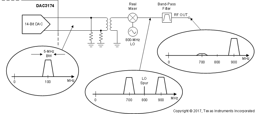
A single-carrier, WCDMA-modulated waveform of 5-MHz bandwidth must be created. The WCDMA signal is modulated up to a 900-MHz carrier using a real mixer. A real mixer creates two images of the signal about the carrier frequency and some bleed-through of the local oscillator (LO); therefore, a band-pass filter is used to filter out the undesired signal image and the local oscillator.
8.2.2 Detailed Design Procedure
The data pattern file that represents the desired 5-MHz, single-carrier, WCDMA signal is created with a pattern generation. Figure 56 shows the DAC3174 being clocked by an FPGA. The data pattern file is generated with the 5-MHz, WCDMA signal centered at an intermediate frequency of 100 MHz, and a local oscillator of 800 MHz is used to upconvert the modulated signal to 900 MHz. The real mixer creates an image of the desired signal centered about 700 MHz, and there is also a LO feedthrough spur present at 800 MHz. Figure 57 illustrates a band-pass filter following the mixer that is required to remove the lower image of the signal and the LO feedthrough spur.
 Figure 57. Signal Spectrum in a Real IF Transmitter
The choice of the intermediate frequency has an impact on the design of the 900-MHz bandpass filter. The band-pass filter passes the WCDMA signal image that is centered at 900 MHz, but provides significant attenuation of the local oscillator feedthrough and the signal image. The distance between the signal and the image is equal to twice the intermediate frequency. If the intermediate frequency is too low, the image gets too close to the signal; therefore, a higher-order band-pass filter with steep rolloff is required. If the intermediate frequency is too high, the image is further away from the signal, but the signal is too far out towards the end of the Nyquist zone, and the sinx/x distortion becomes an issue. Centering the DAC output signal at an intermediate frequency of 100 MHz is a good, balanced choice in this example, and makes the design of the band-pass filter reasonably easy.
The DAC3174 does not have an interpolation option, so the data rate for the sample data are the same rate as the sample rate to the DAC3174. In this case, choose a sample rate of 500 MSPS (a commonly used telecommunications sample rate), so that the sample data rate into the DAC3174 is also 500 MSPS.
8.2.3 Application Curve
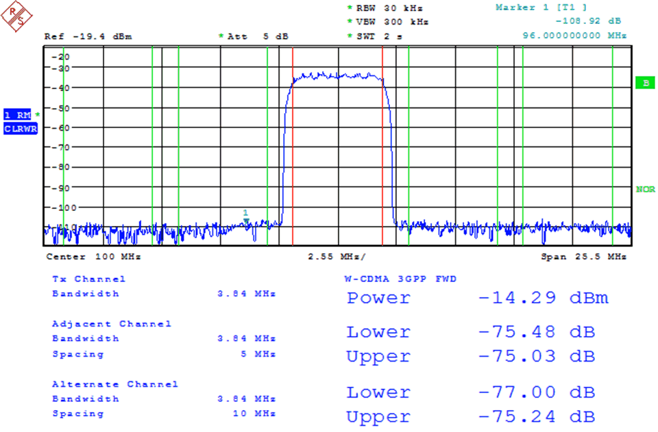
Figure 58 shows the DAC output ACPR of a single-carrier, WCDMA-modulated signal centered at an intermediate frequency of 100 MHz.
 Figure 58. Single-Carrier, WCDMA Signal ACPR at 100 MHz