SLAS751D March 2011 – September 2015 DAC34H84
PRODUCTION DATA.
- 1 Features
- 2 Applications
- 3 Description
- 4 Revision History
- 5 Pin Configuration and Functions
-
6 Specifications
- 6.1 Absolute Maximum Ratings
- 6.2 ESD Ratings
- 6.3 Recommended Operating Conditions
- 6.4 Thermal Information
- 6.5 Electrical Characteristics - DC Specifications
- 6.6 Electrical Characteristics - Digital Specifications
- 6.7 Electrical Characteristics - AC Specifications
- 6.8 Timing Requirements - Digital Specifications
- 6.9 Switching Characteristics - AC Specifications
- 6.10 Typical Characteristics
-
7 Detailed Description
- 7.1 Overview
- 7.2 Functional Block Diagram
- 7.3
Feature Description
- 7.3.1 Serial Interface
- 7.3.2 Data Interface
- 7.3.3 Data Format
- 7.3.4 Input FIFO
- 7.3.5 FIFO Modes of Operation
- 7.3.6 Clocking Modes
- 7.3.7 FIR Filters
- 7.3.8 Complex Signal Mixer
- 7.3.9 Quadrature Modulation Correction (QMC)
- 7.3.10 Temperature Sensor
- 7.3.11 Data Pattern Checker
- 7.3.12 Parity Check Test
- 7.3.13 DAC34H84 Alarm Monitoring
- 7.3.14 LVPECL Inputs
- 7.3.15 LVDS Inputs
- 7.3.16 CMOS Digital Inputs
- 7.3.17 Reference Operation
- 7.3.18 DAC Transfer Function
- 7.3.19 Analog Current Outputs
- 7.4 Device Functional Modes
- 7.5 Programming
- 7.6 Register Map
- 8 Application and Implementation
- 9 Power Supply Recommendations
- 10Layout
- 11Device and Documentation Support
- 12Mechanical, Packaging, and Orderable Information
Package Options
Mechanical Data (Package|Pins)
- ZAY|196
Thermal pad, mechanical data (Package|Pins)
Orderable Information
10 Layout
10.1 Layout Guidelines
The design of the PCB is critical to achieve the full performance of the DAC34H84 device. Defining the PCB stackup should be the first step in the board design. Experience has shown that at least six layers are required to adequately route all required signals to and from the device. Each signal routing layer must have an adjacent solid ground plane to control signal return paths to have minimal loop areas and to achieve controlled impedances for microstrip and stripline routing. Power planes must also have adjacent solid ground planes to control supply return paths. Minimizing the space between supply and ground planes improves performance by increasing the distributed decoupling.
Although the DAC34H84 device consists of both analog and digital circuitry, TI highly recommends solid ground planes that encompass the device and its input and output signal paths. TI does not recommend split ground planes that divide the analog and digital portions of the device. Split ground planes may improve performance if a nearby, noisy, digital device is corrupting the ground reference of the analog signal path. When split ground planes are employed, one must carefully control the supply return paths and keep the paths on top of their respective ground reference planes.
Quality analog output signals and input conversion clock signal path layout is required for full dynamic performance. Symmetry of the differential signal paths and discrete components in the path is mandatory, and symmetrical shunt-oriented components should have a common grounding via. The high frequency requirements of the analog output and clock signal paths necessitate using differential routing with controlled impedances and minimizing signal path stubs (including vias) when possible.
Coupling onto or between the clock and output signals paths should be avoided using any isolation techniques available including distance isolation, orientation planning to prevent field coupling of components like inductors and transformers, and providing well coupled reference planes. Via stitching around the clock signal path and the input analog signal path provides a quiet ground reference for the critical signal paths and reduces noise coupling onto these paths. Sensitive signal traces must not cross other signal traces or power routing on adjacent PCB layers, rather a ground plane must separate the traces. If necessary, the traces should cross at 90° angles to minimize crosstalk.
The substrate (dielectric) material requirements of the PCB are largely influenced by the speed and length of the high speed serial lanes. Affordable and common FR4 varieties are adequate in most cases.
Coupling of ambient signals into the signal path is reduced by providing quiet, close reference planes and by maintaining signal path symmetry to ensure the coupled noise is common-mode. Faraday caging may be used in very noise environment and high dynamic range applications to isolate the signal path.
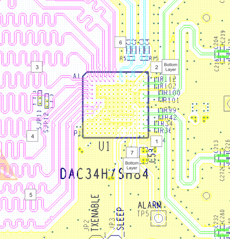
The following layout guidelines correspond to the layout shown in Figure 97.
- DAC output termination resistors should be placed as close to the output pins as possible to provide a DC path to ground and set the source impedance matching.
- For DAC on-chip PLL clocking mode, if the external loop filter is not used, leave the loop filter pin floating without any board routing nearby. Signals coupling to this node may cause clock mixing spurs in the DAC output.
- Route the high speed LVDS lanes as impedance-controlled, tightly-coupled, differential traces.
- Maintain a solid ground plane under the LVDS lanes without any ground plane splits.
- Simulation of the LVDS channel with DAC34H84 IBIS model is recommended to verify good eye opening of the data patterns.
- Keep the OSTR signal routing away from the DACCLK routing to reduce coupling.
- Keep routing for RBIAS short, for instance a resistor can be placed on the board directly connecting the RBIAS pin to the ground layer.
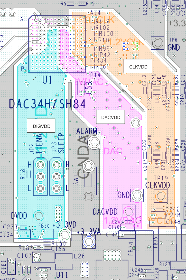
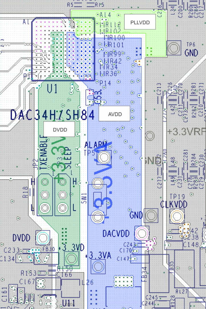
The following layout guidelines correspond to the layouts shown in Figure 98 and Figure 99.
- Noise power supplies should be routed away from clean supplies. Use two power plane layers, preferably with a ground layer in between.
- As shown in Figure 98 and Figure 99, both layers three and four are designated for power supply planes. The DAC analog powers are all in the same layer to avoid coupling with each other, and the planes are copied from layer three to layer four for double the copper coverage area.
- Decoupling capacitors should be placed as close to the supply pins as possible. For instance, a capacitor can be placed on the bottom of the board directly connecting the supply pin to a ground layer.
10.1.1 Assembly
Information regarding the package and assembly of the ZAY package version of the DAC34H84 can be found at the end of the data sheet and also on the following application note: SPRAA99
10.2 Layout Examples
 Figure 97. Top Layer of DAC34H84 Layout Showing High Speed Signals such as LVDS Bus, DACCLK, OSTR, and DAC Outputs. Layout Example from TSW3085EVM Rev D
 Figure 98. Third Layer of DAC34H84 Layout Showing Power Layers. Layout Example from DAC34H84EVM Rev H
 Figure 99. Sixth Layer of DAC34H84 Layout Showing Power Layers. Layout Example from DAC34H84EVM Rev H