SLAS528B August 2017 – January 2018 DAC5672A
PRODUCTION DATA.
- 1 Features
- 2 Applications
- 3 Description
- 4 Revision History
- 5 Pin Configuration and Functions
-
6 Specifications
- 6.1 Absolute Maximum Ratings
- 6.2 ESD Ratings
- 6.3 Recommended Operating Conditions
- 6.4 Thermal Information
- 6.5 Electrical Characteristics
- 6.6 Electrical Characteristics
- 6.7 Electrical Characteristics: AC Characteristics
- 6.8 Electrical Characteristics: Digital Characteristics
- 6.9 Switching Characteristics
- 6.10 Typical Characteristics
- 7 Detailed Description
- 8 Application and Implementation
- 9 Power Supply Recommendations
- 10Layout
- 11Device and Documentation Support
- 12Mechanical, Packaging, and Orderable Information
Package Options
Mechanical Data (Package|Pins)
- PFB|48
Thermal pad, mechanical data (Package|Pins)
- PFB|48
Orderable Information
1 Features
- 14-Bit Dual Transmit Digital-to-Analog Converter (DAC)
- 275 MSPS Update Rate
- Single-Supply: 3 V to 3.6 V
- High Spurious-Free Dynamic Range (SFDR): 84 dBc at 5 MHz
- High Third-Order Two-Tone Intermodulation (IMD3): 79 dBc at 15.1 MHz and 16.1 MHz
- WCDMA Adjacent Channel Leakage Ratio (ACLR): 78 dB at Baseband
- WCDMA ACLR: 73 dB at 30.72 MHz
- Independent or Single Resistor Gain Control
- Dual or Interleaved Data
- On-Chip 1.2-V Reference
- Low Power: 330 mW
- Power-Down Mode: 9 mW
- Package: 48-Pin Thin-Quad Flat Pack (TQFP)
2 Applications
- Cellular Base Transceiver Station Transmit Channel
- CDMA: W-CDMA, CDMA2000, IS-95
- TDMA: GSM, IS-136, EDGE and UWC-136
- Medical and Test Instrumentation
- Arbitrary Waveform Generators (ARB)
- Direct Digital Synthesis (DDS)
- Cable Modem Termination System (CMTS)
3 Description
The DAC5672A device is a monolithic, dual-channel, 14-bit, high-speed DAC with on-chip voltage reference.
Operating with update rates of up to 275 MSPS, the DAC5672A offers exceptional dynamic performance, tight-gain, and offset matching characteristics that make the device well-suited in I/Q baseband or direct IF communication applications.
Each DAC has a high-impedance, differential-current output, suitable for single-ended or differential analog-output configurations. External resistors allow scaling the full-scale output current for each DAC separately or together, typically between 2 mA and 20 mA. An accurate on-chip voltage reference is temperature-compensated and delivers a stable 1.2-V reference voltage. Optionally, an external reference may be used.
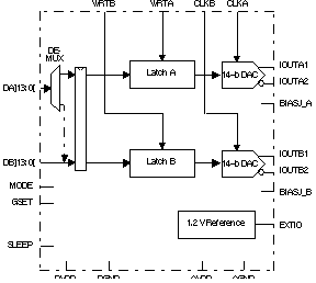
The DAC5672A has two, 14-bit, parallel input ports with separate clocks and data latches. For flexibility, the DAC5672A supports multiplexed data for each DAC on one port when operating in the interleaved mode.
The DAC5672A is specifically designed for a differential transformer-coupled output with a 50-Ω doubly-terminated load. For a 20-mA full-scale output current, a 4:1 impedance ratio (resulting in an output power of 4 dBm) and 1:1 impedance ratio transformer (–2 dBm output power) are supported.
The DAC5672A is available in a 48-pin TQFP package. Pin compatibility between family members provides 12-bit (DAC5662) and 14-bit (DAC5672A) resolutions. Furthermore, the DAC5672A is pin compatible to the DAC2904 and AD9767 dual DACs. The device is characterized for operation over the industrial temperature range of –40°C to 85°C.
- For all available packages, see the orderable addendum at the end of the data sheet.
Functional Block Diagram

4 Revision History
Changes from A Revision (May 2009) to B Revision
- Added Device Information table Go
- Added Temperature Coefficients Offset Drift and Gain Drift to Electrical Characteristics section Go
- Added Feature Description sectionGo
- Added fDATA = 200 MSPS, fOUT = 1 MHz to Power Supply in the Electrical Characteristics sectionGo
- Changed Dual-Bus Data Interface and Timing in Programming sectionGo
- Added 3.3 MAX and 0.8 MAX to Digital Input in Electrical Characteristics sectionGo
- Deleted Available Options tableGo
- Reformatted pinout diagram and pin table in Pin Configuration and Functions sectionGo
- Added ESD Ratings table Go
- Added Recommended Operating Conditions table Go
- Added Thermal Information table Go
- Changed formatting of Table 1Go
- Added Application Information and Typical Application sectionsGo
- Added Power Supply Recommendations section Go
- Added Layout section Go
Changes from * Revision (September 2007) to A Revision