SBAS337E April 2005 – March 2018 DAC7811
PRODUCTION DATA.
- 1 Features
- 2 Applications
- 3 Description
- 4 Revision History
- 5 Pin Configuration and Functions
- 6 Specifications
- 7 Detailed Description
- 8 Application and Implementation
- 9 Power Supply Recommendations
- 10Layout
- 11Device and Documentation Support
- 12Mechanical, Packaging, and Orderable Information
Package Options
Mechanical Data (Package|Pins)
- DGS|10
Thermal pad, mechanical data (Package|Pins)
Orderable Information
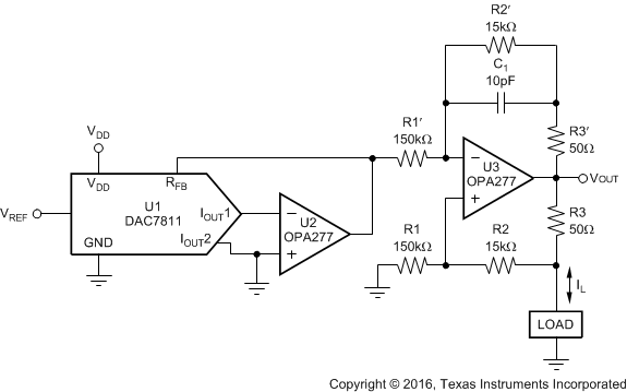
8.1.5 Programmable Current Source Circuit
A DAC7811 can be integrated into the circuit in Figure 31 to implement an improved Howland current pump for precise voltage to current conversions. Bidirectional current flow and high voltage compliance are two features of the circuit. With a matched resistor network, the load current of the circuit is shown by Equation 3:

The value of R3 in Equation 3 can be reduced to increase the output current drive of U3. U3 can drive ±20mA in both directions with voltage compliance limited up to 15V by the U3 voltage supply. Elimination of the circuit compensation capacitor C1 in the circuit is not suggested as a result of the change in the output impedance ZO, according to Equation 4:

As shown in Equation 4, with matched resistors, ZO is infinite and the circuit is optimum for use as a current source. However, if unmatched resistors are used, ZO is positive or negative with negative output impedance being a potential cause of oscillation. Therefore, by incorporating C1 into the circuit, possible oscillation problems are eliminated. The value of C1 can be determined for critical applications; for most applications, however, a value of several pF is suggested.
 Figure 31. Programmable Bidirectional Current Source Circuit