SLAS464C December   2006  – January 2018 DAC8560

PRODUCTION DATA.  

  1. Features
  2. Applications
  3. Description
    1.     Device Images
      1.      Functional Block Diagram
  4. Revision History
  5. Pin Configuration and Functions
    1.     Pin Functions
  6. Specifications
    1. 6.1  Absolute Maximum Ratings
    2. 6.2  ESD Ratings
    3. 6.3  Recommended Operating Conditions
    4. 6.4  Thermal Information
    5. 6.5  Electrical Characteristics
    6. 6.6  Timing Requirements
    7. 6.7  Typical Characteristics: Internal Reference
    8. 6.8  Typical Characteristics: DAC at VDD = 5 V
    9. 6.9  Typical Characteristics: DAC at VDD = 3.6 V
    10. 6.10 Typical Characteristics: DAC at VDD = 2.7 V
  7. Detailed Description
    1. 7.1 Overview
    2. 7.2 Functional Block Diagram
    3. 7.3 Feature Description
      1. 7.3.1 Digital-to-Analog Converter (DAC)
      2. 7.3.2 Resistor String
      3. 7.3.3 Output Amplifier
      4. 7.3.4 DAC Noise Performance
      5. 7.3.5 Internal Reference
        1. 7.3.5.1 Enable/Disable Internal Reference
        2. 7.3.5.2 Internal Reference Load
          1. 7.3.5.2.1 Supply Voltage
          2. 7.3.5.2.2 Temperature Drift
          3. 7.3.5.2.3 Noise Performance
          4. 7.3.5.2.4 Load Regulation
          5. 7.3.5.2.5 Long-Term Stability
          6. 7.3.5.2.6 Thermal Hysteresis
    4. 7.4 Device Functional Modes
      1. 7.4.1 Power-Down Modes
    5. 7.5 Programming
      1. 7.5.1 Serial Interface
      2. 7.5.2 Input Shift Register
      3. 7.5.3 SYNC Interrupt
      4. 7.5.4 Power-On Reset
    6. 7.6 Register Maps
      1. 7.6.1 Write Sequence for Disabling the DAC8560 Internal Reference
        1. Table 1. Write Sequence for Disabling the DAC8560 Internal Reference
      2. 7.6.2 Enabling the DAC8560 Internal Reference (Write Sequence 1 of 2)
        1. Table 2. Enabling the DAC8560 Internal Reference (Write Sequence 1 of 2)
      3. 7.6.3 Enabling the DAC8560 Internal Reference (Write Sequence 2 of 2)
        1. Table 3. Enabling the DAC8560 Internal Reference (Write Sequence 2 of 2)
      4. 7.6.4 DAC8560 Data Input Register Format
        1. Table 4. DAC8560 Data Input Register Format
  8. Application and Implementation
    1. 8.1 Application Information
    2. 8.2 Typical Applications
      1. 8.2.1 Design Requirements
      2. 8.2.2 Detailed Design Procedure or Bipolar Operation > ±VREF
        1. 8.2.2.1 Bipolar Operation Greater Than ±VREF
          1. 8.2.2.1.1 Passive Component Selection
          2. 8.2.2.1.2 Amplifier Selection
        2. 8.2.2.2 Microprocessor Interfacing
          1. 8.2.2.2.1 DAC8560 to 8051 Interface
          2. 8.2.2.2.2 DAC8560 to Microwire Interface
          3. 8.2.2.2.3 DAC8560 to 68HC11 Interface
      3. 8.2.3 Application Curves
  9. Power Supply Recommendations
  10. 10Layout
    1. 10.1 Layout Guidelines
    2. 10.2 Layout Example
  11. 11Device and Documentation Support
    1. 11.1 Documentation Support
      1. 11.1.1 Related Documentation
    2. 11.2 Receiving Notification of Documentation Updates
    3. 11.3 Community Resource
    4. 11.4 Trademarks
    5. 11.5 Electrostatic Discharge Caution
    6. 11.6 Glossary
  12. 12Mechanical, Packaging, and Orderable Information

Package Options

Mechanical Data (Package|Pins)
Thermal pad, mechanical data (Package|Pins)
Orderable Information

Internal Reference Load

The DAC8560 internal reference does not require an external load capacitor for stability because it is stable with any capacitive load. However, for improved noise performance, TI recommends an external load capacitor of 150 nF or larger connected to the VREF output. Figure 66 shows the typical connections required for operation of the DAC8560 internal reference. A supply bypass capacitor at the VDD input is also recommended.
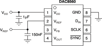
DAC8560 ai_int_ref_las464.gifFigure 66. Typical Connections for Operating the DAC8560 Internal Reference