SLAS464C December 2006 – January 2018 DAC8560
PRODUCTION DATA.
- 1 Features
- 2 Applications
- 3 Description
- 4 Revision History
- 5 Pin Configuration and Functions
-
6 Specifications
- 6.1 Absolute Maximum Ratings
- 6.2 ESD Ratings
- 6.3 Recommended Operating Conditions
- 6.4 Thermal Information
- 6.5 Electrical Characteristics
- 6.6 Timing Requirements
- 6.7 Typical Characteristics: Internal Reference
- 6.8 Typical Characteristics: DAC at VDD = 5 V
- 6.9 Typical Characteristics: DAC at VDD = 3.6 V
- 6.10 Typical Characteristics: DAC at VDD = 2.7 V
-
7 Detailed Description
- 7.1 Overview
- 7.2 Functional Block Diagram
- 7.3 Feature Description
- 7.4 Device Functional Modes
- 7.5 Programming
- 7.6 Register Maps
- 8 Application and Implementation
- 9 Power Supply Recommendations
- 10Layout
- 11Device and Documentation Support
- 12Mechanical, Packaging, and Orderable Information
Package Options
Mechanical Data (Package|Pins)
- DGK|8
Thermal pad, mechanical data (Package|Pins)
- DGK|8
Orderable Information
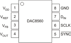
5 Pin Configuration and Functions
DGK Package
8-Pin VSSOP
Top View

Pin Functions
| PIN | I/O | DESCRIPTION | |
|---|---|---|---|
| NO. | NAME | ||
| 1 | VDD | PWR | Power supply input, 2.7 V to 5.5 V |
| 2 | VREF | I/O | Reference voltage input/output |
| 3 | VFB | I | Feedback connection for the output amplifier. For voltage output operation, tie to VOUT externally. |
| 4 | VOUT | O | Analog output voltage from DAC. The output amplifier has rail-to-rail operation. |
| 5 | SYNC | I | Level-triggered control input (active LOW). This is the frame synchronization signal for the input data. When SYNC goes LOW, it enables the input shift register, and data is sampled on subsequent falling clock edges. The DAC output updates following the 24th clock. If SYNC is taken HIGH before the 24th clock edge, the rising edge of SYNC acts as an interrupt, and the write sequence is ignored by the DAC8560. Schmitt-Trigger logic input. |
| 6 | SCLK | I | Serial clock input, Schmitt-Trigger logic input. |
| 7 | DIN | I | Serial data input. Data is clocked into the 24-bit input shift register on each falling edge of the serial clock input. Schmitt-Trigger logic input. |
| 8 | GND | GND | Ground reference point for all circuitry on the device. |