SLASE36A March 2014 – May 2016 DDC1128
PRODUCTION DATA.
- 1Features
- 2Applications
- 3Description
- 4Revision History
- 5Device and Documentation Support
- 6Mechanical, Packaging, and Orderable Information
Package Options
Mechanical Data (Package|Pins)
- ZKL|192
Thermal pad, mechanical data (Package|Pins)
Orderable Information
1 Features
- Single-Chip Solution to Directly Measure
128 Low-Level Currents - Proven High-Precision, True Integrating Architecture with 100% Charge Collection
- Easy Upgrade for Existing DDC Family Applications
- Low Power: 3 mW/channel at 3 kSPS
- Extremely Linear:
INL = ±0.025% of Reading ±1 ppm of FSR - Low Noise: 6.3 ppm of FSR
- Adjustable Full-Scale Range
- Adjustable Speed
- Data Rates up to 6 kSPS with 20-bit Performance
- Integration Times as low as 160 μs
- Daisy-Chainable Serial Interface
- In-Package Bypass Capacitors Simplify PCB Design Area and Design Complexity
2 Applications
- CT Scanner DAS
- Photodiode Sensors
- X-Ray Detection Systems
3 Description
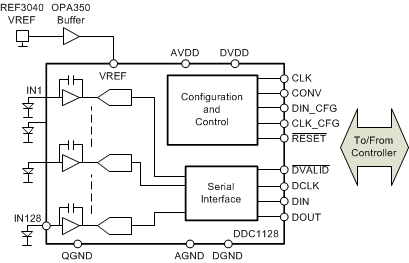
The DDC1128 is a 20-bit, 128-channel, current-input analog-to-digital (A/D) converter. It combines both current-to-voltage and A/D conversion so that 128 separate low-level current output devices, such as photodiodes, can be directly connected to its inputs and digitized.
For each of the 128 inputs, the DDC1128 uses the proven dual switched integrator front-end. This configuration allows for continuous current integration: while one integrator is being digitized by the onboard A/D converter, the other is integrating the input current. This architecture provides both a stable offset and a loss-less collection of the input current. Adjustable integration times range from 160μs to 1s, allowing currents from fAs to μAs to be continuously measured with outstanding precision.
The DDC1128 has a serial interface designed for daisy-chaining in multi-device systems. Simply connect the output of one device to the input of the next to create the chain. Common clocking feeds all the devices in the chain so that the digital overhead in a multi-DDC1128 system is minimal.
The DDC1128 operates from a +5 V analog supply and a 2.7 V to 3.6 V digital supply, it is specified from 0°C to 70°C operating temperature and it is available in a 9 x 9 mm2 192-ball BGA, which includes on board bypass capacitors to help minimize the external component requirements and further reduce board space.
To request a full data sheet or other design resources: request DDC1128
Device Information
| ORDER NUMBER | PACKAGE | BODY SIZE |
|---|---|---|
| DDC1128 | NFBGA (192) | 9.00 mm x 9.00 mm |
SPACER
Simplified Schematic
