SLASED4B March 2016 – May 2016 DDC2256A
PRODUCTION DATA.
- 1Features
- 2Applications
- 3Description
- 4Revision History
- 5Device and Documentation Support
- 6Mechanical, Packaging, and Orderable Information
Package Options
Refer to the PDF data sheet for device specific package drawings
Mechanical Data (Package|Pins)
- ZZF|323
Thermal pad, mechanical data (Package|Pins)
Orderable Information
1 Features
- Single-Chip Solution to Directly Measure 256 Low-Level Currents Simultaneously
- User Adjustable Full-Scale Range
- Adjustable Speed with Integration Times as Low as 58.8 µs (17 KSPS per channel) with 24 bit Resolution
- Power Dissipation as Low as 1.7mW/channel
- Integral Linearity: ±0.025% of Reading ±1 ppm of Full Scale Reading (all channels active)
- Low Noise
- 24 bit ADC
- No Charge Loss and Simultaneous Sampling
- On-board Temperature Sensor
- In-Package Bypass Capacitors and Reference Buffer to Reduce PCB Area and Design Complexity
- Serial LVDS and CMOS Output Interface Option
2 Applications
- CT Scanner Data Acquisition System
- Photodiode Sensors
- X-ray Detection Systems
- Optical Fiber Power Monitoring
- Mutichannel Current/Voltage Instrumentation
3 Description
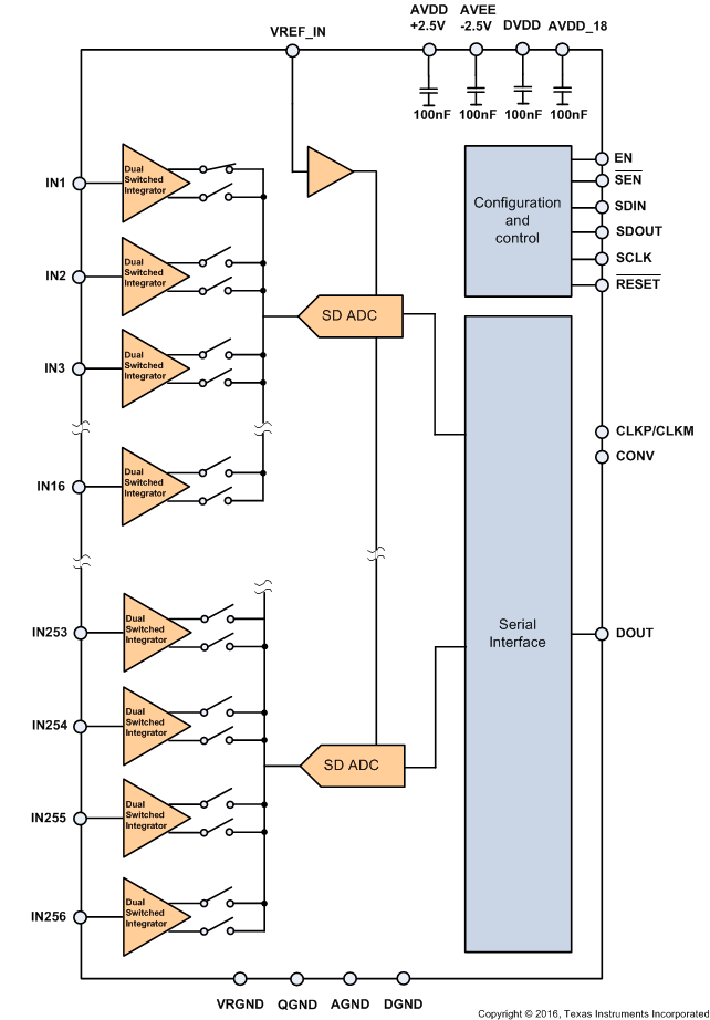
The DDC2256A is a 24-bit, 256-channel, current-input analog-to-digital (A/D) converter. It combines both current-to-voltage integration and A/D conversion so that 256 individual low-level current output devices, such as photodiodes, can be directly connected to its inputs and digitized in parallel (simultaneously).
For each of the inputs, the DDC2256A has one low noise/low power integrator designed to capture all the charge from the sensor. The integration time is adjustable from 58.8μs to 100 ms, allowing currents from fA to uA to be continuously measured with outstanding precision. The outputs of the integrators are digitized by sixteen 24-bit low power ADCs and all the resulting data is output over a single LVDS serial interface pair designed to minimize noise coupling in environments with high channel count.
The DDC2256A operates from ±2.5-V analog supply, 1.8-V analog supply (AVDD_18) and 1.8-V digital supply (DVDD). The device is specified from 0°C to 70°C operating temperature and available in a 14 x 16 mm2 323-ball 0.8 mm-pitch BGA. Finally, the on board reference buffer and bypass capacitors help minimize the external component requirements and further reduce board space.
To request a full data sheet or other design resources: request DDC2256A
Device Information (1)
| PART NUMBER | PACKAGE | BODY SIZE (NOM) |
|---|---|---|
| DDC2256A | NFBGA (323) | 16.0 mm x 14.0 mm |
- For all available packages, see the orderable addendum at the end of the data sheet.
Block Diagram
