DLPS013G April 2010 – January 2019 DLP5500
PRODUCTION DATA.
- 1 Features
- 2 Applications
- 3 Description
- 4 Revision History
- 5 Description (continued)
- 6 Pin Configuration and Functions
-
7 Specifications
- 7.1 Absolute Maximum Ratings
- 7.2 Storage Conditions
- 7.3 ESD Ratings
- 7.4 Recommended Operating Conditions
- 7.5 Thermal Information
- 7.6 Electrical Characteristics
- 7.7 Timing Requirements
- 7.8 System Mounting Interface Loads
- 7.9 Micromirror Array Physical Characteristics
- 7.10 Micromirror Array Optical Characteristics
- 7.11 Window Characteristics
- 7.12 Chipset Component Usage Specification
- 8 Detailed Description
- 9 Application and Implementation
- 10Power Supply Recommendations
- 11Layout
- 12Device and Documentation Support
- 13Mechanical, Packaging, and Orderable Information
Package Options
Mechanical Data (Package|Pins)
- FYA|149
Thermal pad, mechanical data (Package|Pins)
Orderable Information
7.6 Electrical Characteristics
over operating free-air temperature range (unless otherwise noted)| PARAMETER | TEST CONDITIONS | MIN | TYP | MAX | UNIT | ||
|---|---|---|---|---|---|---|---|
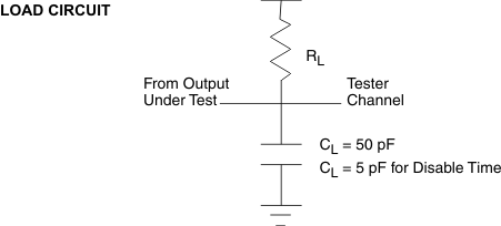
| VOH | High-level output voltage(1), See Figure 2 | VCC = 3.0 V, | IOH = –20 mA | 2.4 | V | ||
| VOL | Low-level output voltage(1), See Figure 2 | VCC = 3.6 V, | IOL = 15 mA | 0.4 | V | ||
| IOZ | High impedance output current(1) | VCC = 3.6 V | 10 | µA | |||
| IIL | Low-level input current(1) | VCC = 3.6 V, | VI = 0 V | –60 | µA | ||
| IIH | High-level input current(1) | VCC = 3.6 V, | VI = VCC | 200 | µA | ||
| ICC | Current into VCC pin | VCC = 3.6 V, | 750 | mA | |||
| ICCI | Current into VOFFSET pin(2) | VCCI = 3.6 V | 450 | mA | |||
| ICC2 | Current into VCC2 pin | VCC2 = 8.75V | 25 | mA | |||
| ZIN | Internal Differential Impedance | 95 | 105 | Ω | |||
| ZLINE | Line Differential Impedance (PWB or Trace) | 90 | 100 | 110 | Ω | ||
| CI | Input capacitance(1) | f = 1 MHz | 10 | pF | |||
| CO | Output capacitance(1) | f = 1 MHz | 10 | pF | |||
| CIM | Input capacitance for MBRST[0:15] pins | f = 1 MHz | 160 | 210 | pF | ||
(1) Applies to LVCMOS pins only
(2) Exceeding the maximum allowable absolute voltage difference between VCC and VCCI may result in excess current draw. (Refer to Absolute Maximum Ratings for details)
