DLPS013G April 2010 – January 2019 DLP5500
PRODUCTION DATA.
- 1 Features
- 2 Applications
- 3 Description
- 4 Revision History
- 5 Description (continued)
- 6 Pin Configuration and Functions
-
7 Specifications
- 7.1 Absolute Maximum Ratings
- 7.2 Storage Conditions
- 7.3 ESD Ratings
- 7.4 Recommended Operating Conditions
- 7.5 Thermal Information
- 7.6 Electrical Characteristics
- 7.7 Timing Requirements
- 7.8 System Mounting Interface Loads
- 7.9 Micromirror Array Physical Characteristics
- 7.10 Micromirror Array Optical Characteristics
- 7.11 Window Characteristics
- 7.12 Chipset Component Usage Specification
- 8 Detailed Description
- 9 Application and Implementation
- 10Power Supply Recommendations
- 11Layout
- 12Device and Documentation Support
- 13Mechanical, Packaging, and Orderable Information
Package Options
Mechanical Data (Package|Pins)
- FYA|149
Thermal pad, mechanical data (Package|Pins)
Orderable Information
7.7 Timing Requirements
over operating free-air temperature range (unless otherwise noted)| MIN | NOM | MAX | UNIT | ||
|---|---|---|---|---|---|
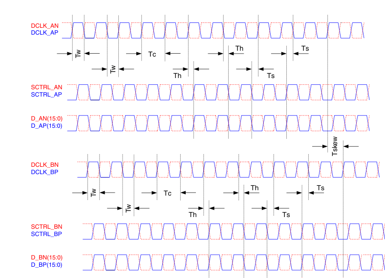
| LVDS TIMING PARAMETERS (See Figure 9) | |||||
| tc | Clock Cycle DLCK_A or DCLKC_B | 5 | ns | ||
| tw | Pulse Width DCLK_A or DCLK_B | 2.5 | ns | ||
| ts | Setup Time, D_A[0:15] before DCLK_A | .35 | ns | ||
| ts | Setup Time, D_B[0:15] before DCLK_B | .35 | ns | ||
| th | Hold Time, D_A[0:15] after DCLK_A | .35 | ns | ||
| th | Hold Time, D_B[0:15] after DCLK_B | .35 | ns | ||
| tskew | Channel B relative to Channel A | –1.25 | 1.25 | ns | |
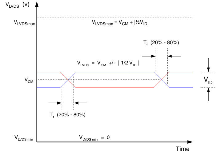
| LVDS WAVEFORM REQUIREMENTS(See Figure 6) | |||||
| |VID| | Input Differential Voltage (absolute difference) | 100 | 400 | 600 | mV |
| VCM | Common Mode Voltage | 1200 | mV | ||
| VLVDS | LVDS Voltage | 0 | 2000 | mV | |
| tr | Rise Time (20% to 80%) | 100 | 400 | ps | |
| tr | Fall Time (80% to 20%) | 100 | 400 | ps | |
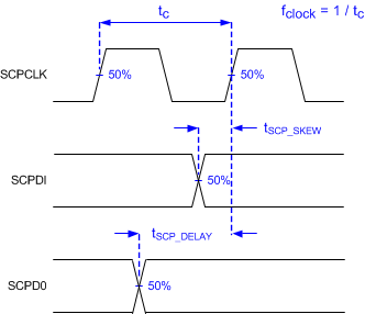
| SERIAL CONTROL BUS TIMING PARAMETERS(See Figure 3 and Figure 4) | |||||
| fSCP_CLK | SCP Clock Frequency | 50 | 500 | kHz | |
| tSCP_SKEW | Time between valid SCP_DI and rising edge of SCP_CLK | –300 | 300 | ns | |
| tSCP_DELAY | Time between valid SCP_DO and rising edge of SCP_CLK | 2600 | ns | ||
| tSCP_EN | Time between falling edge of SCP_EN and the first rising edge of SCP_CLK | 30 | ns | ||
| tr_SCP | Rise time for SCP signals | 200 | ns | ||
| tfP | Fall time for SCP signals | 200 | ns | ||
 Figure 4. Serial Communications Bus Waveform Requirements
 .png)
Refer to LVDS Interface section of the Recommended Operating Conditions.
Refer to Pin Configuration and Functions for list of LVDS pins.
Figure 5. LVDS Voltage Definitions (References) 
Not to scale.
Refer to LVDS Interface section of the Recommended Operating Conditions.
Figure 6. LVDS Waveform Requirements 
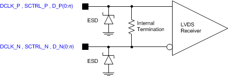
Refer to LVDS Interface section of the Recommended Operating Conditions.
Refer to Pin Configuration and Functions for list of LVDS pins.
Figure 7. LVDS Equivalent Input Circuit 
Not to scale.
Refer to the Timing Requirements.
Refer to Pin Configuration and Functions for list of LVDS pins and SCP pins.
Figure 8. Rise Time and Fall Time  Figure 9. LVDS Timing Waveforms